DEMO9S08JM16 Freescale Semiconductor, DEMO9S08JM16 Datasheet - Page 247
DEMO9S08JM16
Manufacturer Part Number
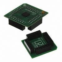
DEMO9S08JM16
Description
BOARD DEMO FOR JM16 FAMI
Manufacturer
Freescale Semiconductor
Type
MCUr
Datasheets
1.DEMO9S08JM16.pdf
(47 pages)
2.DEMO9S08JM16.pdf
(5 pages)
3.DEMO9S08JM16.pdf
(4 pages)
4.DEMO9S08JM16.pdf
(386 pages)
Specifications of DEMO9S08JM16
Contents
Board with Daughter card, Cable, Documentation, Mini-AB USB Kit
Processor To Be Evaluated
MC9S08JM16
Data Bus Width
8 bit
Interface Type
USB
Silicon Manufacturer
Freescale
Core Architecture
HCS08
Core Sub-architecture
HCS08
Silicon Core Number
MC9S08
Silicon Family Name
Flexis - S08JM
Rohs Compliant
Yes
For Use With/related Products
MC9S08JM16
Lead Free Status / RoHS Status
Lead free / RoHS Compliant


Freescale Semiconductor
SPIMODE
MODFEN
BIDIROE
SPISWAI
Reset
SPMIE
SPC0
Field
7
6
4
3
1
0
W
R
SPMIE
SPI Match Interrupt Enable — This is the interrupt enable for the SPI receive data buffer hardware match
(SPMF) function.
0 Interrupts from SPMF inhibited (use polling).
1 When SPMF = 1, requests a hardware interrupt.
SPI 8- or 16-bit Mode — This bit allows the user to select either an 8-bit or 16-bit SPI data transmission length.
In master mode, a change of this bit will abort a transmission in progress, force the SPI system into idle state,
and reset all status bits in the SPIxS register. Refer to section
details.
0 8-bit SPI shift register, match register, and buffers.
1 16-bit SPI shift register, match register, and buffers.
Master Mode-Fault Function Enable — When the SPI is configured for slave mode, this bit has no meaning or
effect. (The SS pin is the slave select input.) In master mode, this bit determines how the SS pin is used (refer to
Table 15-2
0 Mode fault function disabled, master SS pin reverts to general-purpose I/O not controlled by SPI
1 Mode fault function enabled, master SS pin acts as the mode fault input or the slave select output
Bidirectional Mode Output Enable — When bidirectional mode is enabled by SPI pin control 0 (SPC0) = 1,
BIDIROE determines whether the SPI data output driver is enabled to the single bidirectional SPI I/O pin.
Depending on whether the SPI is configured as a master or a slave, it uses either the MOSI (MOMI) or MISO
(SISO) pin, respectively, as the single SPI data I/O pin. When SPC0 = 0, BIDIROE has no meaning or effect.
0 Output driver disabled so SPI data I/O pin acts as an input
1 SPI I/O pin enabled as an output
SPI Stop in Wait Mode — This bit is used for power conservation while in wait.
0 SPI clocks continue to operate in wait mode
1 SPI clocks stop when the MCU enters wait mode
SPI Pin Control 0 — This bit enables bidirectional pin configurations as shown in
0 SPI uses separate pins for data input and data output.
1 SPI configured for single-wire bidirectional operation.
0
7
= Unimplemented or Reserved
for details)
SPIMODE
0
6
Table 15-3. SPIxC2 Register Field Descriptions
Figure 15-6. SPI Control Register 2 (SPIxC2)
MC9S08JM16 Series Data Sheet, Rev. 2
0
0
5
MODFEN
0
4
Description
BIDIROE
3
0
Section 15.4.4, “Data Transmission
Serial Peripheral Interface (S08SPI16V1)
0
0
2
Table
SPISWAI
15-4.
0
1
Length,” for
SPC0
0
0
247
Related parts for DEMO9S08JM16
Image
Part Number
Description
Manufacturer
Datasheet
Request
R

Part Number:
Description:
Manufacturer:
Freescale Semiconductor, Inc
Datasheet:
Part Number:
Description:
Manufacturer:
Freescale Semiconductor, Inc
Datasheet:
Part Number:
Description:
Manufacturer:
Freescale Semiconductor, Inc
Datasheet:
Part Number:
Description:
Manufacturer:
Freescale Semiconductor, Inc
Datasheet:
Part Number:
Description:
Manufacturer:
Freescale Semiconductor, Inc
Datasheet:
Part Number:
Description:
Manufacturer:
Freescale Semiconductor, Inc
Datasheet:
Part Number:
Description:
Manufacturer:
Freescale Semiconductor, Inc
Datasheet:
Part Number:
Description:
Manufacturer:
Freescale Semiconductor, Inc
Datasheet:
Part Number:
Description:
Manufacturer:
Freescale Semiconductor, Inc
Datasheet:
Part Number:
Description:
Manufacturer:
Freescale Semiconductor, Inc
Datasheet:
Part Number:
Description:
Manufacturer:
Freescale Semiconductor, Inc
Datasheet:
Part Number:
Description:
Manufacturer:
Freescale Semiconductor, Inc
Datasheet:
Part Number:
Description:
Manufacturer:
Freescale Semiconductor, Inc
Datasheet:
Part Number:
Description:
Manufacturer:
Freescale Semiconductor, Inc
Datasheet:
Part Number:
Description:
Manufacturer:
Freescale Semiconductor, Inc
Datasheet: