DEMO9S08JM16 Freescale Semiconductor, DEMO9S08JM16 Datasheet - Page 55
DEMO9S08JM16
Manufacturer Part Number
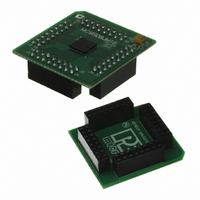
DEMO9S08JM16
Description
BOARD DEMO FOR JM16 FAMI
Manufacturer
Freescale Semiconductor
Type
MCUr
Datasheets
1.DEMO9S08JM16.pdf
(47 pages)
2.DEMO9S08JM16.pdf
(5 pages)
3.DEMO9S08JM16.pdf
(4 pages)
4.DEMO9S08JM16.pdf
(386 pages)
Specifications of DEMO9S08JM16
Contents
Board with Daughter card, Cable, Documentation, Mini-AB USB Kit
Processor To Be Evaluated
MC9S08JM16
Data Bus Width
8 bit
Interface Type
USB
Silicon Manufacturer
Freescale
Core Architecture
HCS08
Core Sub-architecture
HCS08
Silicon Core Number
MC9S08
Silicon Family Name
Flexis - S08JM
Rohs Compliant
Yes
For Use With/related Products
MC9S08JM16
Lead Free Status / RoHS Status
Lead free / RoHS Compliant


4.7.1
Bit 7 of this register is a read-only status flag. Bits 6 through 0 may be read at any time but can be written
only one time. Before any erase or programming operations are possible, write to this register to set the
frequency of the clock for the nonvolatile memory system within acceptable limits.
Table 4-7
Freescale Semiconductor
Reset
PRDIV8
DIV[5:0]
DIVLD
Field
5:0
7
6
W
R
shows the appropriate values for PRDIV8 and DIV5:DIV0 for selected bus frequencies.
DIVLD
Flash Clock Divider Register (FCDIV)
Divisor Loaded Status Flag — When set, this read-only status flag indicates that the FCDIV register has been
written since reset. Reset clears this bit and the first write to this register causes this bit to become set regardless
of the data written.
0 FCDIV has not been written since reset; erase and program operations disabled for flash.
1 FCDIV has been written since reset; erase and program operations enabled for flash.
Prescale (Divide) Flash Clock by 8
0 Clock input to the flash clock divider is the bus rate clock.
1 Clock input to the flash clock divider is the bus rate clock divided by 8.
Divisor for Flash Clock Divider — The flash clock divider divides the bus rate clock (or the bus rate clock
divided by 8 if PRDIV8 = 1) by the value in the 6-bit DIV5:DIV0 field plus one. The resulting frequency of the
internal flash clock must fall within the range of 200 kHz to 150 kHz for proper flash operations. Program/Erase
timing pulses are one cycle of this internal flash clock which corresponds to a range of 5 μs to 6.7 μs. The
automated programming logic uses an integer number of these pulses to complete an erase or program
operation. See
0
7
= Unimplemented or Reserved
PRDIV8
if PRDIV8 = 1 – f
Equation
0
6
if PRDIV8 = 0 – f
Figure 4-5. Flash Clock Divider Register (FCDIV)
Table 4-6. FCDIV Register Field Descriptions
4-1,
MC9S08JM16 Series Data Sheet, Rev. 2
DIV5
Equation
0
5
FCLK
FCLK
= f
4-2, and
= f
Bus
DIV4
Bus
0
4
÷ (8 × ([DIV5:DIV0] + 1))
Table
÷ ([DIV5:DIV0] + 1)
Description
4-6.
DIV3
3
0
DIV2
0
2
DIV1
0
1
Chapter 4 Memory
Eqn. 4-1
Eqn. 4-2
DIV0
0
0
55
Related parts for DEMO9S08JM16
Image
Part Number
Description
Manufacturer
Datasheet
Request
R

Part Number:
Description:
Manufacturer:
Freescale Semiconductor, Inc
Datasheet:
Part Number:
Description:
Manufacturer:
Freescale Semiconductor, Inc
Datasheet:
Part Number:
Description:
Manufacturer:
Freescale Semiconductor, Inc
Datasheet:
Part Number:
Description:
Manufacturer:
Freescale Semiconductor, Inc
Datasheet:
Part Number:
Description:
Manufacturer:
Freescale Semiconductor, Inc
Datasheet:
Part Number:
Description:
Manufacturer:
Freescale Semiconductor, Inc
Datasheet:
Part Number:
Description:
Manufacturer:
Freescale Semiconductor, Inc
Datasheet:
Part Number:
Description:
Manufacturer:
Freescale Semiconductor, Inc
Datasheet:
Part Number:
Description:
Manufacturer:
Freescale Semiconductor, Inc
Datasheet:
Part Number:
Description:
Manufacturer:
Freescale Semiconductor, Inc
Datasheet:
Part Number:
Description:
Manufacturer:
Freescale Semiconductor, Inc
Datasheet:
Part Number:
Description:
Manufacturer:
Freescale Semiconductor, Inc
Datasheet:
Part Number:
Description:
Manufacturer:
Freescale Semiconductor, Inc
Datasheet:
Part Number:
Description:
Manufacturer:
Freescale Semiconductor, Inc
Datasheet:
Part Number:
Description:
Manufacturer:
Freescale Semiconductor, Inc
Datasheet: