C8051F360DK Silicon Laboratories Inc, C8051F360DK Datasheet - Page 8
C8051F360DK
Manufacturer Part Number
C8051F360DK
Description
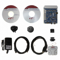
KIT DEV FOR C8051F360 FAMILY
Manufacturer
Silicon Laboratories Inc
Type
MCUr
Specifications of C8051F360DK
Contents
Evaluation Board, Power Supply, USB Cables, Adapter and Documentation
Processor To Be Evaluated
C8051F36x
Interface Type
USB
Lead Free Status / RoHS Status
Lead free / RoHS Compliant
For Use With/related Products
C8051F360, F361, F362, F363, F364, F365, F366, F367, F368, F369
Lead Free Status / Rohs Status
Lead free / RoHS Compliant
Other names
336-1410


List of Figures
1. System Overview
2. Absolute Maximum Ratings
3. Global Electrical Characteristics
4. Pinout and Package Definitions
5. 10-Bit ADC (ADC0, C8051F360/1/2/6/7/8/9)
6. 10-Bit Current Mode DAC (IDA0, C8051F360/1/2/6/7/8/9)
7. Voltage Reference (C8051F360/1/2/6/7/8/9)
8. Comparators
C8051F360/1/2/3/4/5/6/7/8/9
8
Figure 1.1. C8051F360/3 Block Diagram ................................................................. 20
Figure 1.2. C8051F361/4/6/8 Block Diagram ........................................................... 21
Figure 1.3. C8051F362/5/7/9 Block Diagram ........................................................... 21
Figure 1.4. Comparison of Peak MCU Execution Speeds ....................................... 22
Figure 1.5. On-Chip Clock and Reset ......................................................................23
Figure 1.6. On-Board Memory Map ......................................................................... 24
Figure 1.7. Development/In-System Debug Diagram .............................................. 25
Figure 1.8. Digital Crossbar Diagram (Port 0 to Port 3) ........................................... 26
Figure 1.9. PCA Block Diagram ............................................................................... 27
Figure 1.10. PCA Block Diagram .............................................................................27
Figure 1.11. 10-Bit ADC Block Diagram ................................................................... 28
Figure 1.12. Comparator0 Block Diagram ................................................................ 29
Figure 1.13. Comparator1 Block Diagram ................................................................ 30
Figure 1.14. IDA0 Functional Block Diagram ........................................................... 31
Figure 4.1. TQFP-48 Pinout Diagram (Top View) .................................................... 39
Figure 4.2. TQFP-48 Package Diagram ................................................................... 40
Figure 4.3. LQFP-32 Pinout Diagram (Top View) .................................................... 41
Figure 4.4. LQFP-32 Package Diagram ................................................................... 42
Figure 4.5. QFN-28 Pinout Diagram (Top View) ...................................................... 43
Figure 4.6. QFN-28 Package Drawing ..................................................................... 44
Figure 4.7. Typical QFN-28 Landing Diagram ......................................................... 45
Figure 4.8. QFN-28 Solder Paste Recommendation ............................................... 46
Figure 5.1. ADC0 Functional Block Diagram ........................................................... 47
Figure 5.2. Typical Temperature Sensor Transfer Function .................................... 49
Figure 5.3. Temperature Sensor Error with 1-Point Calibration ............................... 50
Figure 5.4. 10-Bit ADC Track and Conversion Example Timing .............................. 52
Figure 5.5. ADC0 Equivalent Input Circuits .............................................................. 53
Figure 5.6. ADC Window Compare Example: Right-Justified Single-Ended Data ... 60
Figure 5.7. ADC Window Compare Example: Left-Justified Single-Ended Data ..... 60
Figure 5.8. ADC Window Compare Example: Right-Justified Differential Data ....... 61
Figure 5.9. ADC Window Compare Example: Left-Justified Differential Data .......... 61
Figure 6.1. IDA0 Functional Block Diagram ............................................................. 63
Figure 6.2. IDA0 Data Word Mapping ......................................................................64
Figure 7.1. Voltage Reference Functional Block Diagram ....................................... 67
Figure 8.1. Comparator0 Functional Block Diagram ................................................ 70
Rev. 1.0
Related parts for C8051F360DK
Image
Part Number
Description
Manufacturer
Datasheet
Request
R

Part Number:
Description:
SMD/C°/SINGLE-ENDED OUTPUT SILICON OSCILLATOR
Manufacturer:
Silicon Laboratories Inc
Part Number:
Description:
Manufacturer:
Silicon Laboratories Inc
Datasheet:
Part Number:
Description:
N/A N/A/SI4010 AES KEYFOB DEMO WITH LCD RX
Manufacturer:
Silicon Laboratories Inc
Datasheet:
Part Number:
Description:
N/A N/A/SI4010 SIMPLIFIED KEY FOB DEMO WITH LED RX
Manufacturer:
Silicon Laboratories Inc
Datasheet:
Part Number:
Description:
N/A/-40 TO 85 OC/EZLINK MODULE; F930/4432 HIGH BAND (REV E/B1)
Manufacturer:
Silicon Laboratories Inc
Part Number:
Description:
EZLink Module; F930/4432 Low Band (rev e/B1)
Manufacturer:
Silicon Laboratories Inc
Part Number:
Description:
I°/4460 10 DBM RADIO TEST CARD 434 MHZ
Manufacturer:
Silicon Laboratories Inc
Part Number:
Description:
I°/4461 14 DBM RADIO TEST CARD 868 MHZ
Manufacturer:
Silicon Laboratories Inc
Part Number:
Description:
I°/4463 20 DBM RFSWITCH RADIO TEST CARD 460 MHZ
Manufacturer:
Silicon Laboratories Inc
Part Number:
Description:
I°/4463 20 DBM RADIO TEST CARD 868 MHZ
Manufacturer:
Silicon Laboratories Inc
Part Number:
Description:
I°/4463 27 DBM RADIO TEST CARD 868 MHZ
Manufacturer:
Silicon Laboratories Inc
Part Number:
Description:
I°/4463 SKYWORKS 30 DBM RADIO TEST CARD 915 MHZ
Manufacturer:
Silicon Laboratories Inc
Part Number:
Description:
N/A N/A/-40 TO 85 OC/4463 RFMD 30 DBM RADIO TEST CARD 915 MHZ
Manufacturer:
Silicon Laboratories Inc
Part Number:
Description:
I°/4463 20 DBM RADIO TEST CARD 169 MHZ
Manufacturer:
Silicon Laboratories Inc