C8051F360DK Silicon Laboratories Inc, C8051F360DK Datasheet - Page 52
C8051F360DK
Manufacturer Part Number
C8051F360DK
Description
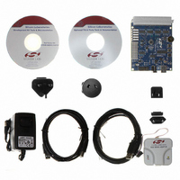
KIT DEV FOR C8051F360 FAMILY
Manufacturer
Silicon Laboratories Inc
Type
MCUr
Specifications of C8051F360DK
Contents
Evaluation Board, Power Supply, USB Cables, Adapter and Documentation
Processor To Be Evaluated
C8051F36x
Interface Type
USB
Lead Free Status / RoHS Status
Lead free / RoHS Compliant
For Use With/related Products
C8051F360, F361, F362, F363, F364, F365, F366, F367, F368, F369
Lead Free Status / Rohs Status
Lead free / RoHS Compliant
Other names
336-1410


C8051F360/1/2/3/4/5/6/7/8/9
5.3.2. Tracking Modes
According to Table 5.1, each ADC0 conversion must be preceded by a minimum tracking time for the con-
verted result to be accurate. The AD0TM bit in register ADC0CN controls the ADC0 track-and-hold mode.
In its default state, the ADC0 input is continuously tracked, except when a conversion is in progress. When
the AD0TM bit is logic ‘1’, ADC0 operates in low-power track-and-hold mode. In this mode, each conver-
sion is preceded by a tracking period of 3 SAR clocks (after the start-of-conversion signal). When the
CNVSTR signal is used to initiate conversions in low-power tracking mode, ADC0 tracks only when
CNVSTR is low; conversion begins on the rising edge of CNVSTR (see Figure 5.4). Tracking can also be
disabled (shutdown) when the device is in low power standby or sleep modes. Low-power track-and-hold
mode is also useful when AMUX settings are frequently changed, due to the settling time requirements
described in Section “5.3.3. Settling Time Requirements” on page 53.
52
(AD0CM[2:0]=000, 001,010
Timer 1, Timer 3 Overflow
Write '1' to AD0BUSY,
(AD0CM[2:0]=100)
Timer 0, Timer 2,
Figure 5.4. 10-Bit ADC Track and Conversion Example Timing
SAR Clocks
SAR Clocks
SAR Clocks
AD0TM=1
AD0TM=0
011, 101)
AD0TM=1
AD0TM=0
CNVSTR
Low Power
or Convert
Low Power
or Convert
Track or
Convert
A. ADC0 Timing for External Trigger Source
Track or Convert
B. ADC0 Timing for Internal Trigger Source
1
1
Track
2
2
Track
Rev. 1.0
3
3
4
4
1
5
5
Convert
2
6
6
3
7
7
4
8
Convert
8
Convert
Convert
5
9
9
6
10 11 12
10 11
7
8
9
13 14
10 11
Low Power Mode
Track
Low Power
Mode
Track
Related parts for C8051F360DK
Image
Part Number
Description
Manufacturer
Datasheet
Request
R

Part Number:
Description:
SMD/C°/SINGLE-ENDED OUTPUT SILICON OSCILLATOR
Manufacturer:
Silicon Laboratories Inc
Part Number:
Description:
Manufacturer:
Silicon Laboratories Inc
Datasheet:
Part Number:
Description:
N/A N/A/SI4010 AES KEYFOB DEMO WITH LCD RX
Manufacturer:
Silicon Laboratories Inc
Datasheet:
Part Number:
Description:
N/A N/A/SI4010 SIMPLIFIED KEY FOB DEMO WITH LED RX
Manufacturer:
Silicon Laboratories Inc
Datasheet:
Part Number:
Description:
N/A/-40 TO 85 OC/EZLINK MODULE; F930/4432 HIGH BAND (REV E/B1)
Manufacturer:
Silicon Laboratories Inc
Part Number:
Description:
EZLink Module; F930/4432 Low Band (rev e/B1)
Manufacturer:
Silicon Laboratories Inc
Part Number:
Description:
I°/4460 10 DBM RADIO TEST CARD 434 MHZ
Manufacturer:
Silicon Laboratories Inc
Part Number:
Description:
I°/4461 14 DBM RADIO TEST CARD 868 MHZ
Manufacturer:
Silicon Laboratories Inc
Part Number:
Description:
I°/4463 20 DBM RFSWITCH RADIO TEST CARD 460 MHZ
Manufacturer:
Silicon Laboratories Inc
Part Number:
Description:
I°/4463 20 DBM RADIO TEST CARD 868 MHZ
Manufacturer:
Silicon Laboratories Inc
Part Number:
Description:
I°/4463 27 DBM RADIO TEST CARD 868 MHZ
Manufacturer:
Silicon Laboratories Inc
Part Number:
Description:
I°/4463 SKYWORKS 30 DBM RADIO TEST CARD 915 MHZ
Manufacturer:
Silicon Laboratories Inc
Part Number:
Description:
N/A N/A/-40 TO 85 OC/4463 RFMD 30 DBM RADIO TEST CARD 915 MHZ
Manufacturer:
Silicon Laboratories Inc
Part Number:
Description:
I°/4463 20 DBM RADIO TEST CARD 169 MHZ
Manufacturer:
Silicon Laboratories Inc