C8051F360DK Silicon Laboratories Inc, C8051F360DK Datasheet - Page 185
C8051F360DK
Manufacturer Part Number
C8051F360DK
Description
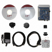
KIT DEV FOR C8051F360 FAMILY
Manufacturer
Silicon Laboratories Inc
Type
MCUr
Specifications of C8051F360DK
Contents
Evaluation Board, Power Supply, USB Cables, Adapter and Documentation
Processor To Be Evaluated
C8051F36x
Interface Type
USB
Lead Free Status / RoHS Status
Lead free / RoHS Compliant
For Use With/related Products
C8051F360, F361, F362, F363, F364, F365, F366, F367, F368, F369
Lead Free Status / Rohs Status
Lead free / RoHS Compliant
Other names
336-1410


17.1. Priority Crossbar Decoder
The Priority Crossbar Decoder (Figure 17.3) assigns a priority to each I/O function, starting at the top with
UART0. When a digital resource is selected, the least-significant unassigned Port pin is assigned to that
resource (excluding UART0, which will be assigned to specific port pins (P0.1 and P0.2 in the
C8051F360/3 devices, P0.4 and P0.5 in the C8051F361/2/4/5/6/7/8/9 devices). If a Port pin is assigned,
the Crossbar skips that pin when assigning the next selected resource. Additionally, the Crossbar will skip
Port pins whose associated bits in the PnSKIP registers are set. The PnSKIP registers allow software to
skip Port pins that are to be used for analog input, dedicated functions, or GPIO.
Important Note on Crossbar Configuration: If a Port pin is claimed by a peripheral without use of the
Crossbar, its corresponding PnSKIP bit should be set. This applies to the port pins associated with the
external oscillator, V
Crossbar skips selected pins as if they were already assigned, and moves to the next unassigned pin.
Figure 17.3 shows the Crossbar Decoder priority with no Port pins skipped (P0SKIP, P1SKIP, P2SKIP,
P3SKIP = 0x00); Figure 17.4 shows the Crossbar Decoder priority with the P1.0 and P1.1 pins skipped
(P1SKIP = 0x03).
TX0
RX0
SDA
SCL
(32- and 28-
PIN I/O
TX0
RX0
SCK
MISO
MOSI
NSS*
CP0
CP0A
CP1
CP1A
/SYSCLK
CEX0
CEX1
CEX2
CEX3
CEX4
CEX5
ECI
T0
T1
SF Signals
SF Signals
(48-pin)
Figure 17.3. Crossbar Priority Decoder with No Pins Skipped
pin)
REF
0
0
1
0
, external CNVSTR signal, IDA0, and any selected ADC or comparator inputs. The
2
0
P0SKIP[0:7]
3
0
P0
4
0
5
0
6
0
7
0
0
0
1
0
2
0
P1SKIP[0:7]
3
0
P1
C8051F360/1/2/3/4/5/6/7/8/9
4
0
Rev. 1.0
5
0
6
0
7
0
(32-pin and 28-pin packages)
(48-pin package)
(*4-Wire SPI Only)
0
0
1
0
2
0
P2SKIP[0:7]
3
0
P2
4
0
5
0
6
0
7
0
0
0
32/48-pin only
available on
1
0
P3.1-P3.4
2
0
P3SKIP[0:7]
3
0
P3
4
0
available
P3.5-P3.7
on 48-pin
5
0
only
6
0
7
0
185
Related parts for C8051F360DK
Image
Part Number
Description
Manufacturer
Datasheet
Request
R

Part Number:
Description:
SMD/C°/SINGLE-ENDED OUTPUT SILICON OSCILLATOR
Manufacturer:
Silicon Laboratories Inc
Part Number:
Description:
Manufacturer:
Silicon Laboratories Inc
Datasheet:
Part Number:
Description:
N/A N/A/SI4010 AES KEYFOB DEMO WITH LCD RX
Manufacturer:
Silicon Laboratories Inc
Datasheet:
Part Number:
Description:
N/A N/A/SI4010 SIMPLIFIED KEY FOB DEMO WITH LED RX
Manufacturer:
Silicon Laboratories Inc
Datasheet:
Part Number:
Description:
N/A/-40 TO 85 OC/EZLINK MODULE; F930/4432 HIGH BAND (REV E/B1)
Manufacturer:
Silicon Laboratories Inc
Part Number:
Description:
EZLink Module; F930/4432 Low Band (rev e/B1)
Manufacturer:
Silicon Laboratories Inc
Part Number:
Description:
I°/4460 10 DBM RADIO TEST CARD 434 MHZ
Manufacturer:
Silicon Laboratories Inc
Part Number:
Description:
I°/4461 14 DBM RADIO TEST CARD 868 MHZ
Manufacturer:
Silicon Laboratories Inc
Part Number:
Description:
I°/4463 20 DBM RFSWITCH RADIO TEST CARD 460 MHZ
Manufacturer:
Silicon Laboratories Inc
Part Number:
Description:
I°/4463 20 DBM RADIO TEST CARD 868 MHZ
Manufacturer:
Silicon Laboratories Inc
Part Number:
Description:
I°/4463 27 DBM RADIO TEST CARD 868 MHZ
Manufacturer:
Silicon Laboratories Inc
Part Number:
Description:
I°/4463 SKYWORKS 30 DBM RADIO TEST CARD 915 MHZ
Manufacturer:
Silicon Laboratories Inc
Part Number:
Description:
N/A N/A/-40 TO 85 OC/4463 RFMD 30 DBM RADIO TEST CARD 915 MHZ
Manufacturer:
Silicon Laboratories Inc
Part Number:
Description:
I°/4463 20 DBM RADIO TEST CARD 169 MHZ
Manufacturer:
Silicon Laboratories Inc