C8051F360DK Silicon Laboratories Inc, C8051F360DK Datasheet - Page 10
C8051F360DK
Manufacturer Part Number
C8051F360DK
Description
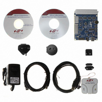
KIT DEV FOR C8051F360 FAMILY
Manufacturer
Silicon Laboratories Inc
Type
MCUr
Specifications of C8051F360DK
Contents
Evaluation Board, Power Supply, USB Cables, Adapter and Documentation
Processor To Be Evaluated
C8051F36x
Interface Type
USB
Lead Free Status / RoHS Status
Lead free / RoHS Compliant
For Use With/related Products
C8051F360, F361, F362, F363, F364, F365, F366, F367, F368, F369
Lead Free Status / Rohs Status
Lead free / RoHS Compliant
Other names
336-1410


C8051F360/1/2/3/4/5/6/7/8/9
18. SMBus
19. UART0
20. Enhanced Serial Peripheral Interface (SPI0)
21. Timers
22. Programmable Counter Array
10
Figure 18.1. SMBus Block Diagram ...................................................................... 202
Figure 18.2. Typical SMBus Configuration ............................................................ 203
Figure 18.3. SMBus Transaction ........................................................................... 204
Figure 18.4. Typical SMBus SCL Generation ........................................................ 207
Figure 18.5. Typical Master Transmitter Sequence ............................................... 213
Figure 18.6. Typical Master Receiver Sequence ................................................... 214
Figure 18.7. Typical Slave Receiver Sequence ..................................................... 215
Figure 18.8. Typical Slave Transmitter Sequence ................................................. 216
Figure 19.1. UART0 Block Diagram ...................................................................... 220
Figure 19.2. UART0 Baud Rate Logic ................................................................... 221
Figure 19.3. UART Interconnect Diagram ............................................................. 222
Figure 19.4. 8-Bit UART Timing Diagram .............................................................. 222
Figure 19.5. 9-Bit UART Timing Diagram .............................................................. 223
Figure 19.6. UART Multi-Processor Mode Interconnect Diagram ......................... 224
Figure 20.1. SPI Block Diagram ............................................................................ 234
Figure 20.2. Multiple-Master Mode Connection Diagram ...................................... 237
Figure 20.3. 3-Wire Single Master and 3-Wire Single Slave Mode
Figure 20.4. 4-Wire Single Master Mode and 4-Wire Slave Mode
Figure 20.5. Master Mode Data/Clock Timing ....................................................... 239
Figure 20.6. Slave Mode Data/Clock Timing (CKPHA = 0) ................................... 240
Figure 20.7. Slave Mode Data/Clock Timing (CKPHA = 1) ................................... 240
Figure 20.8. SPI Master Timing (CKPHA = 0) ....................................................... 244
Figure 20.9. SPI Master Timing (CKPHA = 1) ....................................................... 244
Figure 20.10. SPI Slave Timing (CKPHA = 0) ....................................................... 245
Figure 20.11. SPI Slave Timing (CKPHA = 1) ....................................................... 245
Figure 21.1. T0 Mode 0 Block Diagram ................................................................. 249
Figure 21.2. T0 Mode 2 Block Diagram ................................................................. 250
Figure 21.3. T0 Mode 3 Block Diagram ................................................................. 251
Figure 21.4. Timer 2 16-Bit Mode Block Diagram ................................................. 256
Figure 21.5. Timer 2 8-Bit Mode Block Diagram ................................................... 257
Figure 21.6. Timer 3 16-Bit Mode Block Diagram ................................................. 260
Figure 21.7. Timer 3 8-Bit Mode Block Diagram ................................................... 261
Figure 22.1. PCA Block Diagram ........................................................................... 264
Figure 22.2. PCA Counter/Timer Block Diagram ................................................... 265
Figure 22.3. PCA Interrupt Block Diagram ............................................................ 266
Figure 22.4. PCA Capture Mode Diagram ............................................................. 267
Figure 22.5. PCA Software Timer Mode Diagram ................................................. 268
Figure 22.6. PCA High Speed Output Mode Diagram ........................................... 269
Connection Diagram ......................................................................... 237
Connection Diagram ......................................................................... 237
Rev. 1.0
Related parts for C8051F360DK
Image
Part Number
Description
Manufacturer
Datasheet
Request
R

Part Number:
Description:
SMD/C°/SINGLE-ENDED OUTPUT SILICON OSCILLATOR
Manufacturer:
Silicon Laboratories Inc
Part Number:
Description:
Manufacturer:
Silicon Laboratories Inc
Datasheet:
Part Number:
Description:
N/A N/A/SI4010 AES KEYFOB DEMO WITH LCD RX
Manufacturer:
Silicon Laboratories Inc
Datasheet:
Part Number:
Description:
N/A N/A/SI4010 SIMPLIFIED KEY FOB DEMO WITH LED RX
Manufacturer:
Silicon Laboratories Inc
Datasheet:
Part Number:
Description:
N/A/-40 TO 85 OC/EZLINK MODULE; F930/4432 HIGH BAND (REV E/B1)
Manufacturer:
Silicon Laboratories Inc
Part Number:
Description:
EZLink Module; F930/4432 Low Band (rev e/B1)
Manufacturer:
Silicon Laboratories Inc
Part Number:
Description:
I°/4460 10 DBM RADIO TEST CARD 434 MHZ
Manufacturer:
Silicon Laboratories Inc
Part Number:
Description:
I°/4461 14 DBM RADIO TEST CARD 868 MHZ
Manufacturer:
Silicon Laboratories Inc
Part Number:
Description:
I°/4463 20 DBM RFSWITCH RADIO TEST CARD 460 MHZ
Manufacturer:
Silicon Laboratories Inc
Part Number:
Description:
I°/4463 20 DBM RADIO TEST CARD 868 MHZ
Manufacturer:
Silicon Laboratories Inc
Part Number:
Description:
I°/4463 27 DBM RADIO TEST CARD 868 MHZ
Manufacturer:
Silicon Laboratories Inc
Part Number:
Description:
I°/4463 SKYWORKS 30 DBM RADIO TEST CARD 915 MHZ
Manufacturer:
Silicon Laboratories Inc
Part Number:
Description:
N/A N/A/-40 TO 85 OC/4463 RFMD 30 DBM RADIO TEST CARD 915 MHZ
Manufacturer:
Silicon Laboratories Inc
Part Number:
Description:
I°/4463 20 DBM RADIO TEST CARD 169 MHZ
Manufacturer:
Silicon Laboratories Inc