C8051F360DK Silicon Laboratories Inc, C8051F360DK Datasheet - Page 179
C8051F360DK
Manufacturer Part Number
C8051F360DK
Description
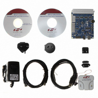
KIT DEV FOR C8051F360 FAMILY
Manufacturer
Silicon Laboratories Inc
Type
MCUr
Specifications of C8051F360DK
Contents
Evaluation Board, Power Supply, USB Cables, Adapter and Documentation
Processor To Be Evaluated
C8051F36x
Interface Type
USB
Lead Free Status / RoHS Status
Lead free / RoHS Compliant
For Use With/related Products
C8051F360, F361, F362, F363, F364, F365, F366, F367, F368, F369
Lead Free Status / Rohs Status
Lead free / RoHS Compliant
Other names
336-1410


16.8.3. Powering on and Initializing the PLL
To set up and use the PLL as the system clock after power-up of the device, the following procedure
should be implemented:
If the PLL characteristics need to be changed when the PLL is already running, the following procedure
should be implemented:
Step 1. Ensure that the reference clock to be used (internal or external) is running and stable.
Step 2. Set the PLLSRC bit (PLL0CN.2) to select the desired clock source for the PLL.
Step 3. Program the Flash read timing bits, FLRT (FLSCL.5–4) to the appropriate value for the
Step 4. Enable power to the PLL by setting PLLPWR (PLL0CN.0) to ‘1’.
Step 5. Program the PLL0DIV register to produce the divided reference frequency to the PLL.
Step 6. Program the PLLLP3–0 bits (PLL0FLT.3–0) to the appropriate range for the divided
Step 7. Program the PLLICO1–0 bits (PLL0FLT.5–4) to the appropriate range for the PLL output
Step 8. Program the PLL0MUL register to the desired clock multiplication factor.
Step 9. Wait at least 5 µs, to provide a fast frequency lock.
Step 10. Enable the PLL by setting PLLEN (PLL0CN.1) to ‘1’.
Step 11. Poll PLLLCK (PLL0CN.4) until it changes from ‘0’ to ‘1’.
Step 12. Switch the System Clock source to the PLL using the CLKSEL register.
Step 1. The system clock should first be switched to either the internal oscillator or an external
Step 2. Ensure that the reference clock to be used for the new PLL setting (internal or external) is
Step 3. Set the PLLSRC bit (PLL0CN.2) to select the new clock source for the PLL.
Step 4. If moving to a faster frequency, program the Flash read timing bits, FLRT (FLSCL.5–4) to
Step 5. Disable the PLL by setting PLLEN (PLL0CN.1) to ‘0’.
Step 6. Program the PLL0DIV register to produce the divided reference frequency to the PLL.
Step 7. Program the PLLLP3–0 bits (PLL0FLT.3–0) to the appropriate range for the divided
Step 8. Program the PLLICO1-0 bits (PLL0FLT.5–4) to the appropriate range for the PLL output
Step 9. Program the PLL0MUL register to the desired clock multiplication factor.
Step 10. Enable the PLL by setting PLLEN (PLL0CN.1) to ‘1’.
Step 11. Poll PLLLCK (PLL0CN.4) until it changes from ‘0’ to ‘1’.
Step 12. Switch the System Clock source to the PLL using the CLKSEL register.
Step 13. If moving to a slower frequency, program the Flash read timing bits, FLRT (FLSCL.5–4)
clock source that is running and stable, using the CLKSEL register.
new clock rate (see Section “13. Flash Memory” on page 135).
reference frequency.
frequency.
running and stable.
the appropriate value for the new clock rate (see Section “13. Flash Memory” on
page 135).
reference frequency.
frequency.
to the appropriate value for the new clock rate (see Section “13. Flash Memory” on
page 135). Important Note: Cache reads, cache writes, and the prefetch engine
should be disabled whenever the FLRT bits are changed to a lower setting.
C8051F360/1/2/3/4/5/6/7/8/9
Rev. 1.0
179
Related parts for C8051F360DK
Image
Part Number
Description
Manufacturer
Datasheet
Request
R

Part Number:
Description:
SMD/C°/SINGLE-ENDED OUTPUT SILICON OSCILLATOR
Manufacturer:
Silicon Laboratories Inc
Part Number:
Description:
Manufacturer:
Silicon Laboratories Inc
Datasheet:
Part Number:
Description:
N/A N/A/SI4010 AES KEYFOB DEMO WITH LCD RX
Manufacturer:
Silicon Laboratories Inc
Datasheet:
Part Number:
Description:
N/A N/A/SI4010 SIMPLIFIED KEY FOB DEMO WITH LED RX
Manufacturer:
Silicon Laboratories Inc
Datasheet:
Part Number:
Description:
N/A/-40 TO 85 OC/EZLINK MODULE; F930/4432 HIGH BAND (REV E/B1)
Manufacturer:
Silicon Laboratories Inc
Part Number:
Description:
EZLink Module; F930/4432 Low Band (rev e/B1)
Manufacturer:
Silicon Laboratories Inc
Part Number:
Description:
I°/4460 10 DBM RADIO TEST CARD 434 MHZ
Manufacturer:
Silicon Laboratories Inc
Part Number:
Description:
I°/4461 14 DBM RADIO TEST CARD 868 MHZ
Manufacturer:
Silicon Laboratories Inc
Part Number:
Description:
I°/4463 20 DBM RFSWITCH RADIO TEST CARD 460 MHZ
Manufacturer:
Silicon Laboratories Inc
Part Number:
Description:
I°/4463 20 DBM RADIO TEST CARD 868 MHZ
Manufacturer:
Silicon Laboratories Inc
Part Number:
Description:
I°/4463 27 DBM RADIO TEST CARD 868 MHZ
Manufacturer:
Silicon Laboratories Inc
Part Number:
Description:
I°/4463 SKYWORKS 30 DBM RADIO TEST CARD 915 MHZ
Manufacturer:
Silicon Laboratories Inc
Part Number:
Description:
N/A N/A/-40 TO 85 OC/4463 RFMD 30 DBM RADIO TEST CARD 915 MHZ
Manufacturer:
Silicon Laboratories Inc
Part Number:
Description:
I°/4463 20 DBM RADIO TEST CARD 169 MHZ
Manufacturer:
Silicon Laboratories Inc