DEMO9S08LC60 Freescale Semiconductor, DEMO9S08LC60 Datasheet - Page 90
DEMO9S08LC60
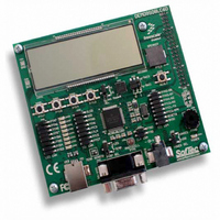
Manufacturer Part Number
DEMO9S08LC60
Description
BOARD DEMO FOR 9S08LC60
Manufacturer
Freescale Semiconductor
Type
MCUr
Datasheets
1.DEMO9S08LC60.pdf
(360 pages)
2.DEMO9S08LC60.pdf
(32 pages)
3.DEMO9S08LC60.pdf
(2 pages)
Specifications of DEMO9S08LC60
Contents
Evaluation Board
Processor To Be Evaluated
MC9S08LC60
Interface Type
RS-232, USB
Silicon Manufacturer
Freescale
Core Architecture
HCS08
Core Sub-architecture
HCS08
Silicon Core Number
MC9S08
Silicon Family Name
S08LC
Rohs Compliant
Yes
For Use With/related Products
MC9S08LC60
Lead Free Status / RoHS Status
Lead free / RoHS Compliant


Chapter 6 Parallel Input/Output
6.2.4.3
An output pin can be selected to have high output drive strength by setting the corresponding bit in the
drive strength select register (PTBDSn). When high drive is selected a pin is capable of sourcing and
sinking greater current. Even though every I/O pin can be selected as high drive, the user must ensure that
the total current source and sink limits for the chip are not exceeded. Drive strength selection is intended
to affect the DC behavior of I/O pins. However, the AC behavior is also affected. High drive allows a pin
to drive a greater load with the same switching speed as a low drive enabled pin into a smaller load.
Because of this the EMC emissions may be affected by enabling pins as high drive.
6.2.5
This section provides information about all registers and control bits associated with the parallel I/O ports.
The parallel I/O registers are located in page zero of the memory map.
Refer to tables in
This section refers to registers and control bits only by their names. A Freescale-provided equate or header
file normally is used to translate these names into the appropriate absolute addresses.
90
PTBDS[7:0]
Reset
Field
7:0
W
R
PTBDS7
Port C Registers
Output Drive Strength Select (
Output Drive Strength Selection for Port B Bits—Each of these control bits selects between low and high output
drive for the associated PTB pin. For port B pins that are configured as inputs, these bits have no effect.
0 Low output drive strength selected for port B bit n.
1 High output drive strength selected for port B bit n.
0
7
Chapter 4,
PTBDS6
Figure 6-17. Drive Strength Selection for Port B (PTBDS)
0
6
MC9S08LC60 Series Data Sheet: Technical Data, Rev. 4
“Memory” for the absolute address assignments for all parallel I/O registers.
Table 6-10. PTBDS Field Descriptions
PTBDS5
0
5
PTBDS4
0
4
PTBDS)
Description
PTBDS3
3
0
PTBDS2
0
2
PTBDS1
Freescale Semiconductor
0
1
PTBDS0
0
0
Related parts for DEMO9S08LC60
Image
Part Number
Description
Manufacturer
Datasheet
Request
R

Part Number:
Description:
Manufacturer:
Freescale Semiconductor, Inc
Datasheet:
Part Number:
Description:
Manufacturer:
Freescale Semiconductor, Inc
Datasheet:
Part Number:
Description:
Manufacturer:
Freescale Semiconductor, Inc
Datasheet:
Part Number:
Description:
Manufacturer:
Freescale Semiconductor, Inc
Datasheet:
Part Number:
Description:
Manufacturer:
Freescale Semiconductor, Inc
Datasheet:
Part Number:
Description:
Manufacturer:
Freescale Semiconductor, Inc
Datasheet:
Part Number:
Description:
Manufacturer:
Freescale Semiconductor, Inc
Datasheet:
Part Number:
Description:
Manufacturer:
Freescale Semiconductor, Inc
Datasheet:
Part Number:
Description:
Manufacturer:
Freescale Semiconductor, Inc
Datasheet:
Part Number:
Description:
Manufacturer:
Freescale Semiconductor, Inc
Datasheet:
Part Number:
Description:
Manufacturer:
Freescale Semiconductor, Inc
Datasheet:
Part Number:
Description:
Manufacturer:
Freescale Semiconductor, Inc
Datasheet:
Part Number:
Description:
Manufacturer:
Freescale Semiconductor, Inc
Datasheet:
Part Number:
Description:
Manufacturer:
Freescale Semiconductor, Inc
Datasheet:
Part Number:
Description:
Manufacturer:
Freescale Semiconductor, Inc
Datasheet: