DEMO9S08LC60 Freescale Semiconductor, DEMO9S08LC60 Datasheet - Page 83
DEMO9S08LC60
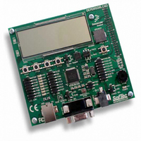
Manufacturer Part Number
DEMO9S08LC60
Description
BOARD DEMO FOR 9S08LC60
Manufacturer
Freescale Semiconductor
Type
MCUr
Datasheets
1.DEMO9S08LC60.pdf
(360 pages)
2.DEMO9S08LC60.pdf
(32 pages)
3.DEMO9S08LC60.pdf
(2 pages)
Specifications of DEMO9S08LC60
Contents
Evaluation Board
Processor To Be Evaluated
MC9S08LC60
Interface Type
RS-232, USB
Silicon Manufacturer
Freescale
Core Architecture
HCS08
Core Sub-architecture
HCS08
Silicon Core Number
MC9S08
Silicon Family Name
S08LC
Rohs Compliant
Yes
For Use With/related Products
MC9S08LC60
Lead Free Status / RoHS Status
Lead free / RoHS Compliant


6.1
Pin behavior following execution of a STOP instruction depends on the stop mode that is entered. An
explanation of pin behavior for the various stop modes follows:
6.2
6.2.1
This section provides information about all registers and control bits associated with the parallel I/O ports.
The parallel I/O registers are located in page zero of the memory map.
Refer to tables in
I/O registers. This section refers to registers and control bits only by their names. A Freescale-provided
equate or header file normally is used to translate these names into the appropriate absolute addresses.
Freescale Semiconductor
•
•
•
In stop1 mode, all internal registers including parallel I/O control and data registers are powered
off. Each of the pins assumes its default reset state (output buffer and internal pullup disabled).
Upon exit from stop1, all pins must be reconfigured the same as if the MCU had been reset.
Stop2 mode is a partial power-down mode, whereby latches maintain the pin state as before the
STOP instruction was executed. CPU register status and the state of I/O registers must be saved in
RAM before the STOP instruction is executed to place the MCU in stop2 mode. Upon recovery
from stop2 mode, before accessing any I/O, the user must examine the state of the PPDF bit in the
SPMSC2 register. If the PPDF bit is 0, I/O must be initialized as if a power on reset had occurred.
If the PPDF bit is 1, I/O data previously stored in RAM, before the STOP instruction was executed,
peripherals previously enabled will require being initialized and restored to their pre-stop
condition. The user must then write a 1 to the PPDACK bit in the SPMSC2 register. Access of pins
is now permitted again in the user’s application program.
In stop3 mode, all pin states are maintained because internal logic stays powered up. Upon
recovery, all pin functions are the same as before entering stop3.
Pin Behavior in Stop Modes
Parallel I/O Registers
Port A Registers
Chapter 3, “Modes of
MC9S08LC60 Series Data Sheet: Technical Data, Rev. 4
Operation” for the absolute address assignments for all parallel
Chapter 6 Parallel Input/Output
83
Related parts for DEMO9S08LC60
Image
Part Number
Description
Manufacturer
Datasheet
Request
R

Part Number:
Description:
Manufacturer:
Freescale Semiconductor, Inc
Datasheet:
Part Number:
Description:
Manufacturer:
Freescale Semiconductor, Inc
Datasheet:
Part Number:
Description:
Manufacturer:
Freescale Semiconductor, Inc
Datasheet:
Part Number:
Description:
Manufacturer:
Freescale Semiconductor, Inc
Datasheet:
Part Number:
Description:
Manufacturer:
Freescale Semiconductor, Inc
Datasheet:
Part Number:
Description:
Manufacturer:
Freescale Semiconductor, Inc
Datasheet:
Part Number:
Description:
Manufacturer:
Freescale Semiconductor, Inc
Datasheet:
Part Number:
Description:
Manufacturer:
Freescale Semiconductor, Inc
Datasheet:
Part Number:
Description:
Manufacturer:
Freescale Semiconductor, Inc
Datasheet:
Part Number:
Description:
Manufacturer:
Freescale Semiconductor, Inc
Datasheet:
Part Number:
Description:
Manufacturer:
Freescale Semiconductor, Inc
Datasheet:
Part Number:
Description:
Manufacturer:
Freescale Semiconductor, Inc
Datasheet:
Part Number:
Description:
Manufacturer:
Freescale Semiconductor, Inc
Datasheet:
Part Number:
Description:
Manufacturer:
Freescale Semiconductor, Inc
Datasheet:
Part Number:
Description:
Manufacturer:
Freescale Semiconductor, Inc
Datasheet: