DEMO9S08LC60 Freescale Semiconductor, DEMO9S08LC60 Datasheet - Page 171
DEMO9S08LC60
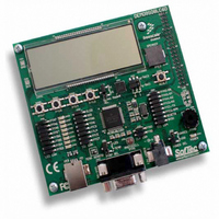
Manufacturer Part Number
DEMO9S08LC60
Description
BOARD DEMO FOR 9S08LC60
Manufacturer
Freescale Semiconductor
Type
MCUr
Datasheets
1.DEMO9S08LC60.pdf
(360 pages)
2.DEMO9S08LC60.pdf
(32 pages)
3.DEMO9S08LC60.pdf
(2 pages)
Specifications of DEMO9S08LC60
Contents
Evaluation Board
Processor To Be Evaluated
MC9S08LC60
Interface Type
RS-232, USB
Silicon Manufacturer
Freescale
Core Architecture
HCS08
Core Sub-architecture
HCS08
Silicon Core Number
MC9S08
Silicon Family Name
S08LC
Rohs Compliant
Yes
For Use With/related Products
MC9S08LC60
Lead Free Status / RoHS Status
Lead free / RoHS Compliant


10.2
The ICG provides multiple options for clock sources. This offers a user great flexibility when making
choices between cost, precision, current draw, and performance. As seen in
of four functional blocks. Each of these is briefly described here and then in more detail in a later section.
10.2.1
The module is intended to be very user friendly with many of the features occurring automatically without
user intervention. To quickly configure the module, go to
Information” and pick an example that best suits the application needs.
Features of the ICG and clock distribution system:
Freescale Semiconductor
•
•
•
•
•
•
•
•
•
Oscillator block — The oscillator block provides means for connecting an external crystal or
resonator. Two frequency ranges are software selectable to allow optimal startup and stability.
Alternatively, the oscillator block can be used to route an external square wave to the system clock.
External sources can provide a very precise clock source. The oscillator is capable of being
configured for low power mode or high amplitude mode as selected by HGO.
Internal reference generator — The internal reference generator consists of two controlled clock
sources. One is designed to be approximately 8 MHz and can be selected as a local clock for the
background debug controller. The other internal reference clock source is typically 243 kHz and
can be trimmed for finer accuracy via software when a precise timed event is input to the MCU.
This provides a highly reliable, low-cost clock source.
Frequency-locked loop — A frequency-locked loop (FLL) stage takes either the internal or
external clock source and multiplies it to a higher frequency. Status bits provide information when
the circuit has achieved lock and when it falls out of lock. Additionally, this block can monitor the
external reference clock and signals whether the clock is valid or not.
Clock select block — The clock select block provides several switch options for connecting
different clock sources to the system clock tree. ICGDCLK is the multiplied clock frequency out
of the FLL, ICGERCLK is the reference clock frequency from the crystal or external clock source,
and FFE (fixed frequency enable) is a control signal used to control the system fixed frequency
clock (XCLK). ICGLCLK is the clock source for the background debug controller (BDC).
Several options for the primary clock source allow a wide range of cost, frequency, and precision
choices:
— 32 kHz–100 kHz crystal or resonator
— 1 MHz–16 MHz crystal or resonator
— External clock
— Internal reference generator
Defaults to self-clocked mode to minimize startup delays
Frequency-locked loop (FLL) generates 8 MHz to 40 MHz (for bus rates up to 20 MHz)
— Uses external or internal clock as reference frequency
Automatic lockout of non-running clock sources
Reset or interrupt on loss of clock or loss of FLL lock
Introduction
Features
MC9S08LC60 Series Data Sheet: Technical Data, Rev. 4
Section 10.6, “Initialization/Application
Chapter 10 Internal Clock Generator (S08ICGV4)
Figure
10-3, the ICG consists
171
Related parts for DEMO9S08LC60
Image
Part Number
Description
Manufacturer
Datasheet
Request
R

Part Number:
Description:
Manufacturer:
Freescale Semiconductor, Inc
Datasheet:
Part Number:
Description:
Manufacturer:
Freescale Semiconductor, Inc
Datasheet:
Part Number:
Description:
Manufacturer:
Freescale Semiconductor, Inc
Datasheet:
Part Number:
Description:
Manufacturer:
Freescale Semiconductor, Inc
Datasheet:
Part Number:
Description:
Manufacturer:
Freescale Semiconductor, Inc
Datasheet:
Part Number:
Description:
Manufacturer:
Freescale Semiconductor, Inc
Datasheet:
Part Number:
Description:
Manufacturer:
Freescale Semiconductor, Inc
Datasheet:
Part Number:
Description:
Manufacturer:
Freescale Semiconductor, Inc
Datasheet:
Part Number:
Description:
Manufacturer:
Freescale Semiconductor, Inc
Datasheet:
Part Number:
Description:
Manufacturer:
Freescale Semiconductor, Inc
Datasheet:
Part Number:
Description:
Manufacturer:
Freescale Semiconductor, Inc
Datasheet:
Part Number:
Description:
Manufacturer:
Freescale Semiconductor, Inc
Datasheet:
Part Number:
Description:
Manufacturer:
Freescale Semiconductor, Inc
Datasheet:
Part Number:
Description:
Manufacturer:
Freescale Semiconductor, Inc
Datasheet:
Part Number:
Description:
Manufacturer:
Freescale Semiconductor, Inc
Datasheet: