PCM18XT0 Microchip Technology, PCM18XT0 Datasheet - Page 471
PCM18XT0
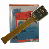
Manufacturer Part Number
PCM18XT0
Description
MODULE PROC PIC18F4685
Manufacturer
Microchip Technology
Datasheet
1.PCM18XT0.pdf
(484 pages)
Specifications of PCM18XT0
Accessory Type
Processor Module
Product
Microcontroller Modules
Core Processor
PIC18F4685
Lead Free Status / RoHS Status
Not applicable / Not applicable
For Use With/related Products
ICE2000
For Use With
ICE2000 - EMULATOR MPLAB-ICE 2000 POD
Lead Free Status / RoHS Status
Lead free / RoHS Compliant, Not applicable / Not applicable


Data EEPROM Memory ................................................... 107
Data Memory ..................................................................... 69
DAW ................................................................................. 384
DC and AC Characteristics .............................................. 455
DC Characteristics ........................................................... 430
DCFSNZ .......................................................................... 385
DECF ............................................................................... 384
DECFSZ ........................................................................... 385
Development Support ...................................................... 415
Device Differences ........................................................... 465
Device Overview .................................................................. 9
Device Reset Timers .......................................................... 47
Direct Addressing ............................................................... 91
Disable Mode ................................................................... 327
E
ECAN Module
© 2009 Microchip Technology Inc.
Associated Registers ............................................... 111
EEADR and EEADRH Registers ............................. 107
EECON1 and EECON2 Registers ........................... 107
Operation During Code-Protect ............................... 110
Protection Against Spurious Write ........................... 110
Reading .................................................................... 109
Use ........................................................................... 110
Write Verify .............................................................. 109
Writing ...................................................................... 109
Access Bank .............................................................. 71
Bank Select Register (BSR) ....................................... 69
Extended Instruction Set ............................................ 93
General Purpose Register File ................................... 71
Map for PIC18F268X/468X ........................................ 70
Special Function Registers ........................................ 72
Power-Down and Supply Current ............................ 422
Supply Voltage ......................................................... 421
Features (table) .......................................................... 11
New Core Features ...................................................... 9
Oscillator Start-up Timer (OST) ................................. 47
PLL Lock Time-out ..................................................... 47
Power-up Timer (PWRT) ........................................... 47
Baud Rate Setting .................................................... 335
Bit Time Partitioning ................................................. 335
Bit Timing Configuration Registers .......................... 340
Calculating T
CAN Interrupts ......................................................... 342
CAN Message Buffers ............................................. 329
338
Acknowledge ................................................... 344
Bus Activity Wake-up ....................................... 344
Bus-Off ............................................................. 344
Code Bits ......................................................... 343
Error ................................................................. 344
Message Error ................................................. 343
Receive ............................................................ 343
Receiver Bus Passive ...................................... 344
Receiver Overflow ........................................... 344
Receiver Warning ............................................ 344
Transmit ........................................................... 343
Transmitter Bus Passive .................................. 344
Transmitter Warning ........................................ 344
Dedicated Receive ........................................... 329
Dedicated Transmit .......................................... 329
Programmable Auto-RTR ................................ 330
Programmable Transmit/Receive .................... 329
Q
, Nominal Bit Rate and Nominal Bit Time
PIC18F2682/2685/4682/4685
Effect on Standard PIC Instructions ................................. 412
Electrical Characteristics ................................................. 419
CAN Message Transmission ................................... 330
CAN Modes of Operation ........................................ 327
CAN Registers ......................................................... 277
Configuration Mode ................................................. 327
Disable Mode ........................................................... 327
Error Detection ........................................................ 341
Error Modes State (diagram) ................................... 342
Error Recognition Mode ........................................... 328
Filter-Mask Truth (table) .......................................... 333
Functional Modes .................................................... 328
Information Processing Time (IPT) .......................... 338
Lengthening a Bit Period ......................................... 339
Listen Only Mode ..................................................... 328
Loopback Mode ....................................................... 328
Message Acceptance Filters and Masks ......... 305, 333
Message Acceptance Mask and
Message Reception ................................................. 332
Normal Mode ........................................................... 327
Oscillator Tolerance ................................................. 340
Overview .................................................................. 275
Phase Buffer Segments ........................................... 338
Programmable TX/RX and Auto-RTR Buffers ......... 297
Programming Time Segments ................................. 340
Propagation Segment .............................................. 338
Sample Point ........................................................... 338
Shortening a Bit Period ............................................ 340
Synchronization ....................................................... 339
Synchronization Segment ........................................ 338
Time Quanta ............................................................ 338
Values for ICODE (table) ......................................... 343
Aborting ........................................................... 330
Initiating ........................................................... 330
Priority ............................................................. 331
Baud Rate ....................................................... 314
Control and Status ........................................... 277
Controller Map ................................................. 322
Dedicated Receive Buffers .............................. 290
Dedicated Transmit Buffers ............................. 284
I/O Control ....................................................... 317
Interrupt ........................................................... 318
Acknowledge ................................................... 341
Bit .................................................................... 341
CRC ................................................................. 341
Error States ..................................................... 341
Form ................................................................ 341
Modes and Counters ....................................... 341
Stuff Bit ............................................................ 341
Mode 0 (Legacy Mode) .................................... 328
Mode 1 (Enhanced Legacy Mode) .................. 328
Mode 2 (Enhanced FIFO Mode) ...................... 329
Filter Operation ................................................ 334
Enhanced FIFO Mode ..................................... 333
Priority ............................................................. 332
Time-Stamping ................................................ 333
Hard ................................................................. 339
Resynchronization ........................................... 339
Rules ............................................................... 339
DS39761C-page 471
Related parts for PCM18XT0
Image
Part Number
Description
Manufacturer
Datasheet
Request
R

Part Number:
Description:
Manufacturer:
Microchip Technology Inc.
Datasheet:
Part Number:
Description:
Manufacturer:
Microchip Technology Inc.
Datasheet:
Part Number:
Description:
Manufacturer:
Microchip Technology Inc.
Datasheet:
Part Number:
Description:
Manufacturer:
Microchip Technology Inc.
Datasheet:
Part Number:
Description:
Manufacturer:
Microchip Technology Inc.
Datasheet:
Part Number:
Description:
Manufacturer:
Microchip Technology Inc.
Datasheet:
Part Number:
Description:
Manufacturer:
Microchip Technology Inc.
Datasheet:
Part Number:
Description:
Manufacturer:
Microchip Technology Inc.
Datasheet: