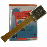
PCM18XT0 Microchip Technology, PCM18XT0 Datasheet - Page 454

PCM18XT0
Manufacturer Part Number
PCM18XT0
Description
MODULE PROC PIC18F4685
Manufacturer
Microchip Technology
Datasheet
1.PCM18XT0.pdf
(484 pages)
Specifications of PCM18XT0
Accessory Type
Processor Module
Product
Microcontroller Modules
Core Processor
PIC18F4685
Lead Free Status / RoHS Status
Not applicable / Not applicable
For Use With/related Products
ICE2000
For Use With
ICE2000 - EMULATOR MPLAB-ICE 2000 POD
Lead Free Status / RoHS Status
Lead free / RoHS Compliant, Not applicable / Not applicable
- Current page: 454 of 484
- Download datasheet (9Mb)
PIC18F2682/2685/4682/4685
FIGURE 27-22:
TABLE 27-25: A/D CONVERSION REQUIREMENTS
DS39761C-page 454
130
131
132
135
136
Note 1:
Param
No.
Note 1:
A/D CLK
A/D DATA
2:
3:
4:
5:
SAMPLE
ADRES
T
T
T
T
T
BSF ADCON0, GO
Symbol
AD
CNV
ACQ
SWC
AMP
ADIF
2:
The time of the A/D clock period is dependent on the device frequency and the T
ADRES register may be read on the following T
The time for the holding capacitor to acquire the “New” input voltage when the voltage changes full scale
after the conversion (AV
50Ω.
On the following cycle of the device clock.
See Section 19.0 “10-Bit Analog-to-Digital Converter (A/D) Module” for minimum conditions when input
voltage has changed more than 1 LSb.
GO
Q4
(1)
If the A/D clock source is selected as RC, a time of T
This allows the SLEEP instruction to be executed.
This is a minimal RC delay (typically 100 ns), which also disconnects the holding capacitor from the analog input.
A/D Clock Period
Conversion Time
(not including acquisition time) (Note 2)
Acquisition Time (Note 3)
Switching Time from Convert → Sample
Amplifier Settling Time (Note 5)
132
A/D CONVERSION TIMING
Characteristic
(Note 2)
DD
9
to AV
PIC18FXXXX
PIC18LFXXXX
PIC18FXXXX
PIC18LFXXXX
8
SS
OLD_DATA
or AV
7
SAMPLING STOPPED
SS
. . .
to AV
CY
is added before the A/D clock starts.
CY
Min
1.4
0.7
1.4
—
—
11
—
DD
1
. . .
cycle.
131
130
). The source impedance (R
(Note 4)
25.0
25.0
Max
2
12
—
—
1
3
(1)
(1)
1
Units
T
μs
μs
μs
μs
μs
μs
AD
T
V
T
A/D RC mode
V
-40°C to +85°C
This may be used if the “new” input
voltage has not changed by more
than 1 LSb (i.e., 5 mV @ 5.12V)
from the last sampled voltage (as
stated on C
OSC
OSC
DD
DD
0
© 2009 Microchip Technology Inc.
= 2.0V;
= 2.0V; A/D RC mode
based, V
based, V
S
AD
) on the input channels is
clock divider.
Conditions
HOLD
DONE
NEW_DATA
REF
REF
).
T
CY
≥ 3.0V
full range
Related parts for PCM18XT0
Image
Part Number
Description
Manufacturer
Datasheet
Request
R

Part Number:
Description:
Manufacturer:
Microchip Technology Inc.
Datasheet:

Part Number:
Description:
Manufacturer:
Microchip Technology Inc.
Datasheet:

Part Number:
Description:
Manufacturer:
Microchip Technology Inc.
Datasheet:

Part Number:
Description:
Manufacturer:
Microchip Technology Inc.
Datasheet:

Part Number:
Description:
Manufacturer:
Microchip Technology Inc.
Datasheet:

Part Number:
Description:
Manufacturer:
Microchip Technology Inc.
Datasheet:

Part Number:
Description:
Manufacturer:
Microchip Technology Inc.
Datasheet:

Part Number:
Description:
Manufacturer:
Microchip Technology Inc.
Datasheet:


