PCM18XT0 Microchip Technology, PCM18XT0 Datasheet - Page 18
PCM18XT0
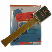
Manufacturer Part Number
PCM18XT0
Description
MODULE PROC PIC18F4685
Manufacturer
Microchip Technology
Datasheet
1.PCM18XT0.pdf
(484 pages)
Specifications of PCM18XT0
Accessory Type
Processor Module
Product
Microcontroller Modules
Core Processor
PIC18F4685
Lead Free Status / RoHS Status
Not applicable / Not applicable
For Use With/related Products
ICE2000
For Use With
ICE2000 - EMULATOR MPLAB-ICE 2000 POD
Lead Free Status / RoHS Status
Lead free / RoHS Compliant, Not applicable / Not applicable


PIC18F2682/2685/4682/4685
TABLE 1-3:
DS39761C-page 18
MCLR/V
OSC1/CLKI/RA7
OSC2/CLKO/RA6
Legend: TTL = TTL compatible input
MCLR
V
RE3
OSC1
CLKI
RA7
OSC2
CLKO
RA6
PP
Pin Name
PP
/RE3
ST = Schmitt Trigger input with CMOS levels
O
= Output
PIC18F4682/4685 PINOUT I/O DESCRIPTIONS
PDIP
13
14
1
Pin Number
QFN
18
32
33
TQFP
18
30
31
Type
Pin
I/O
I/O
O
O
P
I
I
I
I
CMOS
Buffer
Type
TTL
TTL
ST
ST
ST
—
—
Master Clear (input) or programming voltage (input).
Oscillator crystal or external clock input.
Oscillator crystal or clock output.
CMOS = CMOS compatible input or output
I
P
Master Clear (Reset) input. This pin is an
active-low Reset to the device.
Programming voltage input.
Digital input.
Oscillator crystal input or external clock source input.
ST buffer when configured in RC mode;
CMOS otherwise.
External clock source input. Always associated with
pin function OSC1. (See related OSC2/CLKO pin.)
General purpose I/O pin.
Oscillator crystal output. Connects to crystal or
resonator in Crystal Oscillator mode.
In RC mode, OSC2 pin outputs CLKO which has 1/4
the frequency of OSC1 and denotes the instruction
cycle rate.
General purpose I/O pin.
= Input
= Power
Description
© 2009 Microchip Technology Inc.
Related parts for PCM18XT0
Image
Part Number
Description
Manufacturer
Datasheet
Request
R

Part Number:
Description:
Manufacturer:
Microchip Technology Inc.
Datasheet:
Part Number:
Description:
Manufacturer:
Microchip Technology Inc.
Datasheet:
Part Number:
Description:
Manufacturer:
Microchip Technology Inc.
Datasheet:
Part Number:
Description:
Manufacturer:
Microchip Technology Inc.
Datasheet:
Part Number:
Description:
Manufacturer:
Microchip Technology Inc.
Datasheet:
Part Number:
Description:
Manufacturer:
Microchip Technology Inc.
Datasheet:
Part Number:
Description:
Manufacturer:
Microchip Technology Inc.
Datasheet:
Part Number:
Description:
Manufacturer:
Microchip Technology Inc.
Datasheet: