PCM18XT0 Microchip Technology, PCM18XT0 Datasheet - Page 249
PCM18XT0
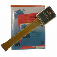
Manufacturer Part Number
PCM18XT0
Description
MODULE PROC PIC18F4685
Manufacturer
Microchip Technology
Datasheet
1.PCM18XT0.pdf
(484 pages)
Specifications of PCM18XT0
Accessory Type
Processor Module
Product
Microcontroller Modules
Core Processor
PIC18F4685
Lead Free Status / RoHS Status
Not applicable / Not applicable
For Use With/related Products
ICE2000
For Use With
ICE2000 - EMULATOR MPLAB-ICE 2000 POD
Lead Free Status / RoHS Status
Lead free / RoHS Compliant, Not applicable / Not applicable


19.0
The Analog-to-Digital (A/D) converter module has
8 inputs for the PIC18F2682/2685 devices and 11 for
the PIC18F4682/4685 devices. This module allows
conversion of an analog input signal to a corresponding
10-bit digital number.
REGISTER 19-1:
© 2009 Microchip Technology Inc.
bit 7
Legend:
R = Readable bit
-n = Value at POR
bit 7-6
bit 5-2
bit 1
bit 0
Note 1:
U-0
—
2:
10-BIT ANALOG-TO-DIGITAL
CONVERTER (A/D) MODULE
These channels are not implemented on PIC18F2682/2685 devices.
Performing a conversion on unimplemented channels will return full-scale measurements.
Unimplemented: Read as ‘0’
CHS3:CHS0: Analog Channel Select bits
0000 = Channel 0 (AN0)
0001 = Channel 1 (AN1)
0010 = Channel 2 (AN2)
0011 = Channel 3 (AN3)
0100 = Channel 4 (AN4)
0101 = Channel 5 (AN5)
0110 = Channel 6 (AN6)
0111 = Channel 7 (AN7)
1000 = Channel 8 (AN8)
1001 = Channel 9 (AN9)
1010 = Channel 10 (AN10)
1011 = Unused
1100 = Unused
1101 = Unused
1110 = Unused
1111 = Unused
GO/DONE: A/D Conversion Status bit
When ADON = 1:
1 = A/D conversion in progress
0 = A/D Idle
ADON: A/D On bit
1 = A/D converter module is enabled
0 = A/D converter module is disabled
U-0
—
ADCON0: A/D CONTROL REGISTER 0
W = Writable bit
‘1’ = Bit is set
R/W-0
CHS3
(1,2)
(1,2)
(1,2)
PIC18F2682/2685/4682/4685
R/W-0
CHS2
U = Unimplemented bit, read as ‘0’
‘0’ = Bit is cleared
R/W-0
CHS1
The module has five registers:
• A/D Result High Register (ADRESH)
• A/D Result Low Register (ADRESL)
• A/D Control Register 0 (ADCON0)
• A/D Control Register 1 (ADCON1)
• A/D Control Register 2 (ADCON2)
The ADCON0 register, shown in Register 19-1, controls
the operation of the A/D module. The ADCON1 register,
shown in Register 19-2, configures the functions of the
port pins. The ADCON2 register, shown in Register 19-3,
configures the A/D clock source, programmed
acquisition time and justification.
R/W-0
CHS0
x = Bit is unknown
GO/DONE
R/W-0
DS39761C-page 249
R/W-0
ADON
bit 0
Related parts for PCM18XT0
Image
Part Number
Description
Manufacturer
Datasheet
Request
R

Part Number:
Description:
Manufacturer:
Microchip Technology Inc.
Datasheet:
Part Number:
Description:
Manufacturer:
Microchip Technology Inc.
Datasheet:
Part Number:
Description:
Manufacturer:
Microchip Technology Inc.
Datasheet:
Part Number:
Description:
Manufacturer:
Microchip Technology Inc.
Datasheet:
Part Number:
Description:
Manufacturer:
Microchip Technology Inc.
Datasheet:
Part Number:
Description:
Manufacturer:
Microchip Technology Inc.
Datasheet:
Part Number:
Description:
Manufacturer:
Microchip Technology Inc.
Datasheet:
Part Number:
Description:
Manufacturer:
Microchip Technology Inc.
Datasheet: