PCM18XT0 Microchip Technology, PCM18XT0 Datasheet - Page 231
PCM18XT0
Manufacturer Part Number
PCM18XT0
Description
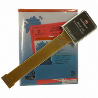
MODULE PROC PIC18F4685
Manufacturer
Microchip Technology
Datasheet
1.PCM18XT0.pdf
(484 pages)
Specifications of PCM18XT0
Accessory Type
Processor Module
Product
Microcontroller Modules
Core Processor
PIC18F4685
Lead Free Status / RoHS Status
Not applicable / Not applicable
For Use With/related Products
ICE2000
For Use With
ICE2000 - EMULATOR MPLAB-ICE 2000 POD
Lead Free Status / RoHS Status
Lead free / RoHS Compliant, Not applicable / Not applicable


REGISTER 18-2:
© 2009 Microchip Technology Inc.
bit 7
Legend:
R = Readable bit
-n = Value at POR
bit 7
bit 6
bit 5
bit 4
bit 3
bit 2
bit 1
bit 0
R/W-0
SPEN
SPEN: Serial Port Enable bit
1 = Serial port enabled (configures RX/DT and TX/CK pins as serial port pins)
0 = Serial port disabled (held in Reset)
RX9: 9-Bit Receive Enable bit
1 = Selects 9-bit reception
0 = Selects 8-bit reception
SREN: Single Receive Enable bit
Asynchronous mode:
Don’t care.
Synchronous mode – Master:
1 = Enables single receive
0 = Disables single receive
This bit is cleared after reception is complete.
Synchronous mode – Slave:
Don’t care.
CREN: Continuous Receive Enable bit
Asynchronous mode:
1 = Enables receiver
0 = Disables receiver
Synchronous mode:
1 = Enables continuous receive until enable bit CREN is cleared (CREN overrides SREN)
0 = Disables continuous receive
ADDEN: Address Detect Enable bit
Asynchronous mode 9-bit (RX9 = 1):
1 = Enables address detection, enables interrupt and loads the receive buffer when RSR<8> is set
0 = Disables address detection, all bytes are received and ninth bit can be used as parity bit
Asynchronous mode 9-bit (RX9 = 0):
Don’t care.
FERR: Framing Error bit
1 = Framing error (can be updated by reading RCREG register and receiving next valid byte)
0 = No framing error
OERR: Overrun Error bit
1 = Overrun error (can be cleared by clearing bit CREN)
0 = No overrun error
RX9D: 9th bit of Received Data
This can be an address/data bit or a parity bit and must be calculated by user firmware.
R/W-0
RX9
RCSTA: RECEIVE STATUS AND CONTROL REGISTER
W = Writable bit
‘1’ = Bit is set
R/W-0
SREN
PIC18F2682/2685/4682/4685
R/W-0
CREN
U = Unimplemented bit, read as ‘0’
‘0’ = Bit is cleared
ADDEN
R/W-0
FERR
R-0
x = Bit is unknown
OERR
R-0
DS39761C-page 231
RX9D
R-x
bit 0
Related parts for PCM18XT0
Image
Part Number
Description
Manufacturer
Datasheet
Request
R

Part Number:
Description:
Manufacturer:
Microchip Technology Inc.
Datasheet:
Part Number:
Description:
Manufacturer:
Microchip Technology Inc.
Datasheet:
Part Number:
Description:
Manufacturer:
Microchip Technology Inc.
Datasheet:
Part Number:
Description:
Manufacturer:
Microchip Technology Inc.
Datasheet:
Part Number:
Description:
Manufacturer:
Microchip Technology Inc.
Datasheet:
Part Number:
Description:
Manufacturer:
Microchip Technology Inc.
Datasheet:
Part Number:
Description:
Manufacturer:
Microchip Technology Inc.
Datasheet:
Part Number:
Description:
Manufacturer:
Microchip Technology Inc.
Datasheet: