PCM18XT0 Microchip Technology, PCM18XT0 Datasheet - Page 161
PCM18XT0
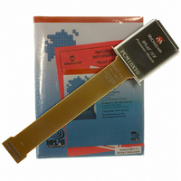
Manufacturer Part Number
PCM18XT0
Description
MODULE PROC PIC18F4685
Manufacturer
Microchip Technology
Datasheet
1.PCM18XT0.pdf
(484 pages)
Specifications of PCM18XT0
Accessory Type
Processor Module
Product
Microcontroller Modules
Core Processor
PIC18F4685
Lead Free Status / RoHS Status
Not applicable / Not applicable
For Use With/related Products
ICE2000
For Use With
ICE2000 - EMULATOR MPLAB-ICE 2000 POD
Lead Free Status / RoHS Status
Lead free / RoHS Compliant, Not applicable / Not applicable


14.0
The Timer3 timer/counter module incorporates these
features:
• Software selectable operation as a 16-bit timer or
• Readable and writable 8-bit registers (TMR3H
• Selectable clock source (internal or external) with
• Interrupt on overflow
• Module Reset on CCP1 Special Event Trigger
REGISTER 14-1:
© 2009 Microchip Technology Inc.
bit 7
Legend:
R = Readable bit
-n = Value at POR
bit 7
bit 6,3
bit 5-4
bit 2
bit 1
bit 0
Note 1:
counter
and TMR3L)
device clock or Timer1 oscillator internal options
R/W-0
RD16
TIMER3 MODULE
Thess bits and the ECCP1 module are available on PIC18F4682/4685 devices only.
RD16: 16-Bit Read/Write Mode Enable bit
1 = Enables register read/write of Timer3 in one 16-bit operation
0 = Enables register read/write of Timer3 in two 8-bit operations
T3ECCP1:T3CCP1: Timer3 and Timer1 to ECCP1/CCP1 Enable bits
1x = Timer3 is the capture/compare clock source for both CCP1 and ECCP1 modules
01 = Timer3 is the capture/compare clock source for ECCP1;
00 = Timer1 is the capture/compare clock source for both CCP1 and ECCP1 modules
T3CKPS1:T3CKPS0: Timer3 Input Clock Prescale Select bits
11 = 1:8 Prescale value
10 = 1:4 Prescale value
01 = 1:2 Prescale value
00 = 1:1 Prescale value
T3SYNC: Timer3 External Clock Input Synchronization Control bit
(Not usable if the device clock comes from Timer1/Timer3.)
When TMR3CS = 1:
1 = Do not synchronize external clock input
0 = Synchronize external clock input
When TMR3CS = 0:
This bit is ignored. Timer3 uses the internal clock when TMR3CS = 0.
TMR3CS: Timer3 Clock Source Select bit
1 = External clock input from Timer1 oscillator or T13CKI (on the rising edge after the first falling edge)
0 = Internal clock (F
TMR3ON: Timer3 On bit
1 = Enables Timer3
0 = Stops Timer3
T3ECCP1
R/W-0
Timer1 is the capture/compare clock source for CCP1
T3CON: TIMER3 CONTROL REGISTER
(1)
W = Writable bit
‘1’ = Bit is set
T3CKPS1
R/W-0
OSC
/4)
PIC18F2682/2685/4682/4685
T3CKPS0
R/W-0
U = Unimplemented bit, read as ‘0’
‘0’ = Bit is cleared
T3CCP1
R/W-0
A simplified block diagram of the Timer3 module is
shown in Figure 14-1. A block diagram of the module’s
operation in Read/Write mode is shown in Figure 14-2.
The Timer3 module is controlled through the T3CON
register (Register 14-1). It also selects the clock source
options
Section 15.1.1
Resources” for more information).
(1)
for
T3SYNC
R/W-0
the
“CCP1
ECCP1/CCP1
(1)
x = Bit is unknown
TMR3CS
Modules
R/W-0
DS39761C-page 161
modules
and
TMR3ON
R/W-0
Timer
bit 0
(see
Related parts for PCM18XT0
Image
Part Number
Description
Manufacturer
Datasheet
Request
R

Part Number:
Description:
Manufacturer:
Microchip Technology Inc.
Datasheet:
Part Number:
Description:
Manufacturer:
Microchip Technology Inc.
Datasheet:
Part Number:
Description:
Manufacturer:
Microchip Technology Inc.
Datasheet:
Part Number:
Description:
Manufacturer:
Microchip Technology Inc.
Datasheet:
Part Number:
Description:
Manufacturer:
Microchip Technology Inc.
Datasheet:
Part Number:
Description:
Manufacturer:
Microchip Technology Inc.
Datasheet:
Part Number:
Description:
Manufacturer:
Microchip Technology Inc.
Datasheet:
Part Number:
Description:
Manufacturer:
Microchip Technology Inc.
Datasheet: