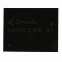
HYB18T1G160BF-5 Qimonda, HYB18T1G160BF-5 Datasheet - Page 9

HYB18T1G160BF-5
Manufacturer Part Number
HYB18T1G160BF-5
Description
IC DDR2 SDRAM 1GBIT 84TFBGA
Manufacturer
Qimonda
Datasheet
1.HYB18T1G800BF-3S.pdf
(74 pages)
Specifications of HYB18T1G160BF-5
Format - Memory
RAM
Memory Type
DDR2 SDRAM
Memory Size
1G (64M x 16)
Speed
200MHz
Interface
Parallel
Voltage - Supply
1.7 V ~ 1.9 V
Operating Temperature
0°C ~ 95°C
Package / Case
84-TFBGA
Lead Free Status / RoHS Status
Lead free / RoHS Compliant
Other names
675-1018-2
- Current page: 9 of 74
- Download datasheet (5Mb)
2
This chapter contains the chip configuration and addressing.
2.1
The chip configuration of a DDR2 SDRAM is listed by function in
columns are explained in
Rev. 1.3, 2007-07
03062006-ZNH8-HURV
Ball#
Clock Signals ×4×8 Organizations
J8
K8
K2
Control Signals ×4×8 Organizations
K7
L7
K3
L8
Address Signals ×4×8 Organizations
L2
L3
L1
Name
CK
CK
CKE
RAS
CAS
WE
CS
BA0
BA1
BA2
Configuration
Chip Configuration for PG-TFBGA-68
Table 8
Ball
Type
I
I
I
I
I
I
I
I
I
I
and
Table 9
Buffer
Type
SSTL
SSTL
SSTL
SSTL
SSTL
SSTL
SSTL
SSTL
SSTL
SSTL
respectively. The ball numbering for the FBGA package is depicted in figures.
Function
Clock Signal CK, CK
Clock Enable
Row Address Strobe (RAS), Column Address Strobe (CAS), Write
Enable (WE)
Chip Select
Bank Address Bus 1:0
Bank Address Bus 2
Note: 1 Gbit components and higher
9
Table
7. The abbreviations used in the Ball# and Buffer Type
Chip Configuration of DDR2 SDRAM
1-Gbit Double-Data-Rate-Two SDRAM
HY[B/I]18T1G[40/80/16]0B[C/F](L/V)
Internet Data Sheet
TABLE 7
Related parts for HYB18T1G160BF-5
Image
Part Number
Description
Manufacturer
Datasheet
Request
R

Part Number:
Description:
BGA
Manufacturer:
Qimonda
Datasheet:

Part Number:
Description:
BGA
Manufacturer:
Qimonda
Datasheet:

Part Number:
Description:
Manufacturer:
Qimonda
Datasheet:

Part Number:
Description:
Manufacturer:
Qimonda
Datasheet:

Part Number:
Description:
DDR2 16Mx16, 667MHz, FBGA84, leadfree
Manufacturer:
Qimonda
Datasheet:

Part Number:
Description:
DDR2 32Mx16, 533MHz, FBGA84, leadfree
Manufacturer:
Qimonda
Datasheet:

Part Number:
Description:
HYB18TC1G160BF-3.71-Gbit DDR2 SDRAM
Manufacturer:
QIMONDA Qimonda AG
Datasheet:

Part Number:
Description:
HYB18TC1G800BF-3S1-Gbit DDR2 SDRAM
Manufacturer:
QIMONDA Qimonda AG
Datasheet:


