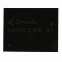
HYB18T1G160BF-5 Qimonda, HYB18T1G160BF-5 Datasheet - Page 57

HYB18T1G160BF-5
Manufacturer Part Number
HYB18T1G160BF-5
Description
IC DDR2 SDRAM 1GBIT 84TFBGA
Manufacturer
Qimonda
Datasheet
1.HYB18T1G800BF-3S.pdf
(74 pages)
Specifications of HYB18T1G160BF-5
Format - Memory
RAM
Memory Type
DDR2 SDRAM
Memory Size
1G (64M x 16)
Speed
200MHz
Interface
Parallel
Voltage - Supply
1.7 V ~ 1.9 V
Operating Temperature
0°C ~ 95°C
Package / Case
84-TFBGA
Lead Free Status / RoHS Status
Lead free / RoHS Compliant
Other names
675-1018-2
1)
2) Timing that is not specified is illegal and after such an event, in order to guarantee proper operation, the DRAM must be powered down
3) Timings are guaranteed with CK/CK differential Slew Rate of 2.0 V/ns. For DQS signals timings are guaranteed with a differential Slew
4) The CK / CK input reference level (for timing reference to CK / CK) is the point at which CK and CK cross. The DQS / DQS, RDQS / RDQS,
5) Inputs are not recognized as valid until
6) The output timing reference voltage level is
7) For each of the terms, if not already an integer, round to the next highest integer.
8) The clock frequency is allowed to change during self-refresh mode or precharge power-down mode.
9) For timing definition, refer to the Component data sheet.
10) Consists of data pin skew and output pattern effects, and p-channel to n-channel variation of the output drivers as well as output Slew Rate
Rev. 1.3, 2007-07
03062006-ZNH8-HURV
Parameter
Data output hold time from DQS
Data hold skew factor
Average periodic refresh Interval
Average periodic refresh Interval
Auto-Refresh to Active/Auto-Refresh
command period
Precharge-All (8 banks) command period
Read preamble
Read postamble
Active bank A to Active bank B command
period
Active bank A to Active bank B command
period
Internal Read to Precharge command delay
Write preamble
Write postamble
Write recovery time for write without Auto-
Precharge
Internal Write to Read command delay
Exit power down to any valid command
(other than NOP or Deselect)
Exit active power-down mode to Read
command (slow exit, lower power)
Exit precharge power-down to any valid
command (other than NOP or Deselect)
Exit Self-Refresh to non-Read command
Exit Self-Refresh to Read command
Write recovery time for write with Auto-
Precharge
V
and then restarted through the specified initialization sequence before normal operation can continue.
Rate of 2.0 V/ns in differential strobe mode and a Slew Rate of 1 V/ns in single ended mode.
input reference level is the crosspoint when in differential strobe mode. The input reference level for signals other than CK/CK, DQS/DQS,
RDQS / RDQS is defined.
the WR parameter stored in the MR.
mis-match between DQS / DQS and associated DQ in any given cycle.
DDQ
= 1.8 V ± 0.1 V;
V
DD
= 1.8 V ±0.1 V.
V
REF
V
stabilizes. During the period before
TT
.
Symbol
t
t
t
t
t
t
t
t
t
t
t
t
t
t
t
t
t
t
t
t
WR
QH
QHS
REFI
REFI
RFC
RP
RPRE
RPST
RRD
RRD
RTP
WPRE
WPST
WR
WTR
XARD
XARDS
XP
XSNR
XSRD
57
DDR2–533
t
—
—
—
127.5
t
0.9
0.40
7.5
7.5
0.25
0.40
15
7.5
2
6 – AL
2
t
200
t
Min.
HP
RP
10
RFC
WR
–
/
+ 1 ×
t
t
+10
CK
QHS
t
V
CK
t
REF
CK
refers to the application clock period. WR refers to
stabilizes, CKE = 0.2 x
1-Gbit Double-Data-Rate-Two SDRAM
HY[B/I]18T1G[40/80/16]0B[C/F](L/V)
Max.
—
400
7.8
3.9
—
—
1.1
0.60
—
—
—
—
0.60
—
—
—
—
—
—
—
—
V
DDQ
Unit
ps
µs
µs
ns
ns
t
t
ns
ns
ns
t
t
ns
ns
t
t
t
ns
t
t
Internet Data Sheet
CK
CK
CK
CK
CK
CK
CK
CK
CK
is recognized as low.
Note
6)
13)14)
15)17)
16)
13)
13)
13)17)
15)21)
18)
19)
20)
20)
21)
1)2)3)4)5)


