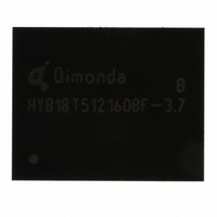
HYB18T1G160BF-5 Qimonda, HYB18T1G160BF-5 Datasheet - Page 34

HYB18T1G160BF-5
Manufacturer Part Number
HYB18T1G160BF-5
Description
IC DDR2 SDRAM 1GBIT 84TFBGA
Manufacturer
Qimonda
Datasheet
1.HYB18T1G800BF-3S.pdf
(74 pages)
Specifications of HYB18T1G160BF-5
Format - Memory
RAM
Memory Type
DDR2 SDRAM
Memory Size
1G (64M x 16)
Speed
200MHz
Interface
Parallel
Voltage - Supply
1.7 V ~ 1.9 V
Operating Temperature
0°C ~ 95°C
Package / Case
84-TFBGA
Lead Free Status / RoHS Status
Lead free / RoHS Compliant
Other names
675-1018-2
5.3
DDR2 SDRAM pin timing are specified for either single ended
or differential mode depending on the setting of the EMRS(1)
“Enable DQS” mode bit; timing advantages of differential
mode are realized in system design. The method by which the
DDR2 SDRAM pin timing are measured is mode dependent.
In single ended mode, timing relationships are measured
relative to the rising or falling edges of DQS crossing at
1) Input waveform timing is referenced to the input signal crossing through the
2) The input signal minimum Slew Rate is to be maintained over the range from
3) AC timings are referenced with input waveforms switching from
Rev. 1.3, 2007-07
03062006-ZNH8-HURV
Symbol
V
V
V
V
Symbol
V
V
V
V
Symbol
V
V
SLEW
IH(dc)
IL(dc)
IH(ac)
IL(ac)
IH(dc)
IL(dc)
IH(ac)
IL(ac)
REF
SWING.MAX
V
transitions.
IL(ac).MAX
for falling edges as shown in
Parameter
DC input logic high
DC input low
AC input logic high
AC input low
DC input logic high
DC input low
AC input logic high
AC input low
Parameter
Condition
Input reference voltage
Input signal maximum peak to peak swing
Input signal minimum Slew Rate
DC & AC Characteristics
Figure 4
V
DC & AC Logic Input Levels for DDR2-667 and DDR2-800
DC & AC Logic Input Levels for DDR2-533 and DDR2-400
REF
DDR2-667, DDR2-800
V
–0.3
V
—
DDR2-533, DDR2-400
V
–0.3
V
—
Min.
Min.
REF
REF
V
REF
REF
.
IL(ac)
34
+ 0.125
+ 0.200
+ 0.125
+ 0.250
to
In differential mode, these timing relationships are measured
relative to the crosspoint of DQS and its complement, DQS.
This distinction in timing methods is verified by design and
characterization but not subject to production test. In single
ended mode, the DQS (and RDQS) signals are internally
disabled and don’t care.
V
IH(ac)
V
V
on the positive transitions and
REF
IH(ac).MIN
level applied to the device under test.
Value
0.5 x
1.0
1.0
Single-ended AC Input Test Conditions
to
1-Gbit Double-Data-Rate-Two SDRAM
V
V
REF
HY[B/I]18T1G[40/80/16]0B[C/F](L/V)
DDQ
Max.
V
V
—
V
Max.
V
V
—
V
DDQ
REF
REF
for rising edges and the range from
DDQ
REF
REF
– 0.125
– 0.200
+ 0.3
- 0.125
- 0.250
+ 0.3
V
IH(ac)
Internet Data Sheet
Unit
V
V
V / ns
to
V
IL(ac)
TABLE 33
TABLE 34
TABLE 35
on the negative
Units
V
V
V
V
Units
V
V
V
V
Note
1)
1)
2)3)
V
REF
to


