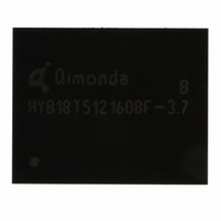
HYB18T1G160BF-5 Qimonda, HYB18T1G160BF-5 Datasheet - Page 3

HYB18T1G160BF-5
Manufacturer Part Number
HYB18T1G160BF-5
Description
IC DDR2 SDRAM 1GBIT 84TFBGA
Manufacturer
Qimonda
Datasheet
1.HYB18T1G800BF-3S.pdf
(74 pages)
Specifications of HYB18T1G160BF-5
Format - Memory
RAM
Memory Type
DDR2 SDRAM
Memory Size
1G (64M x 16)
Speed
200MHz
Interface
Parallel
Voltage - Supply
1.7 V ~ 1.9 V
Operating Temperature
0°C ~ 95°C
Package / Case
84-TFBGA
Lead Free Status / RoHS Status
Lead free / RoHS Compliant
Other names
675-1018-2
1
This chapter gives an overview of the 1-Gbit Double-Data-Rate-Two SDRAM product family and describes its main
characteristics.
1.1
The 1-Gbit Double-data-Rate SDRAM offers the following key features:
• 1.8 V
• DRAM organizations with 4, 8 and 16 data in/outputs
• Double Data Rate architecture: two data transfers per
• Programmable CAS Latency: 3, 4, 5 and 6
• Programmable Burst Length: 4 and 8
• Differential clock inputs (CK and CK)
• Bi-directional, differential data strobes (DQS and DQS) are
• DLL aligns DQ and DQS transitions with clock
• DQS can be disabled for single-ended data strobe
• Commands entered on each positive clock edge, data and
• Data masks (DM) for write data
• Posted CAS by programmable additive latency for better
1) RoHS Compliant Product: Restriction of the use of certain hazardous substances (RoHS) in electrical and electronic equipment as defined
Rev. 1.3, 2007-07
03062006-ZNH8-HURV
Product Type Speed Code
Speed Grade
Max. Clock Frequency
Min. RAS-CAS-Delay
Min. Row Precharge Time
Min. Row Active Time
Min. Row Cycle Time
1.8 V
clock cycle four internal banks for concurrent operation
transmitted / received with data. Edge aligned with read
data and center-aligned with write data
operation
data mask are referenced to both edges of DQS
command and data bus efficiency
in the directive 2002/95/EC issued by the European Parliament and of the Council of 27 January 2003. These substances include mercury,
lead, cadmium, hexavalent chromium, polybrominated biphenyls and polybrominated biphenyl ethers.
±
±
0.1 V Power Supply
0.1 V (SSTL_18) compatible I/O
Overview
Features
@CL6
@CL5
@CL4
@CL3
f
f
f
f
t
t
t
t
CK6
CK5
CK4
CK3
RCD
RP
RAS
RC
–2.5F
DDR2–800D 5–5–5
400
400
266
200
12.5
12.5
45
57.5
3
• Off-Chip-Driver impedance adjustment (OCD) and On-
• Auto-Precharge operation for read and write bursts
• Auto-Refresh, Self-Refresh and power saving Power-
• Average Refresh Period 7.8 µs at a
• Programmable self refresh rate via EMRS2 setting
• Programmable partial array refresh via EMRS2 settings
• DCC enabling via EMRS2 setting
• Full and reduced Strength Data-Output Drivers
• 1K page size for ×4 & ×8, 2K page size for ×16
• Package: P(G)-TFBGA-68 , P(G)-TFBGA-84
• RoHS Compliant Products
• All Speed grades faster than DDR2–400 comply with
Die-Termination (ODT) for better signal quality
Down modes
85 °C, 3.9 µs between 85 °C and 95 °C
and PG-TFBGA-92
DDR2–400 timing specifications when run at a clock rate
of 200 MHz.
–2.5
DDR2–800E 6–6–6
400
333
266
200
15
15
45
60
1-Gbit Double-Data-Rate-Two SDRAM
HY[B/I]18T1G[40/80/16]0B[C/F](L/V)
Performance Tables for –2.5(F)
1)
Internet Data Sheet
T
CASE
lower than
TABLE 1
Unit
—
MHz
MHz
MHz
MHz
ns
ns
ns
ns


