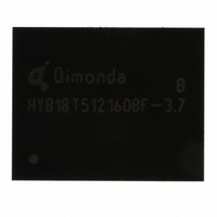
HYB18T1G160BF-5 Qimonda, HYB18T1G160BF-5 Datasheet - Page 54

HYB18T1G160BF-5
Manufacturer Part Number
HYB18T1G160BF-5
Description
IC DDR2 SDRAM 1GBIT 84TFBGA
Manufacturer
Qimonda
Datasheet
1.HYB18T1G800BF-3S.pdf
(74 pages)
Specifications of HYB18T1G160BF-5
Format - Memory
RAM
Memory Type
DDR2 SDRAM
Memory Size
1G (64M x 16)
Speed
200MHz
Interface
Parallel
Voltage - Supply
1.7 V ~ 1.9 V
Operating Temperature
0°C ~ 95°C
Package / Case
84-TFBGA
Lead Free Status / RoHS Status
Lead free / RoHS Compliant
Other names
675-1018-2
26)
27) The Auto-Refresh command interval has be reduced to 3.9 µs when operating the DDR2 DRAM in a temperature range between 85 °C
28) 0 °C≤
29) 85 °C <
30) A maximum of eight Auto-Refresh commands can be posted to any given DDR2 SDRAM device.
31)
32) When the device is operated with input clock jitter, this parameter needs to be derated by the actual
33) When the device is operated with input clock jitter, this parameter needs to be derated by the actual
34) For these parameters, the DDR2 SDRAM device is characterized and verified to support
35)
Rev. 1.3, 2007-07
03062006-ZNH8-HURV
t
1) The pulse duration distortion of on-chip clock circuits, which represents how well the actual
and
2) The worst case push-out of DQS on one transition followed by the worst case pull-in of DQ on the next transition, both of which are
independent of each other, due to data pin skew, output pattern effects, and pchannel to n-channel variation of the output drivers.
and 95 °C.
t
(
driving (
calculation is consistent.
deratings are relative to the SDRAM input clock.) For example, if the measured jitter into a DDR2–667 SDRAM has
and
+
deratings are relative to the SDRAM input clock.) For example, if the measured jitter into a DDR2–667 SDRAM has
and
+
cycles, assuming all input clock jitter specifications are satisfied. For example, the device will support
clock cycles, if all input clock jitter specifications are met. This means: For DDR2–667 5–5–5, of which
t
Tm + 5 is valid even if (Tm + 5 - Tm) is less than 15 ns due to input clock jitter.
t
QHS
RPST
t
nRP
WTR
RPST
t
t
JIT.PER.MAX
JIT.DUTY.MAX
t
t
= RU{
accounts for:
is at lease two clocks (2 x
JIT.PER.MAX
JIT.DUTY.MAX
end point and
), or begins driving (
T
CASE
T
t
RPRE
CASE
t
RP
≤ 85 °C
= 1.1 x
) by measuring the signal at two different voltages. The actual voltage measurement points are not critical as long as the
/
= 0.6 x
≤ 95 °C
= + 93 ps, then
t
CK.AVG
= + 93 ps, then
t
t
RPRE
CK.AVG
t
} = 5, i.e. as long as the input clock jitter specifications are met, Precharge command at Tm and Active command at
CK.AVG
begin point are not referenced to a specific voltage level but specify when the device output is no longer driving
t
RPRE
+ 93 ps = + 2843 ps. (Caution on the MIN/MAX usage!).
+ 93 ps = + 1592 ps. (Caution on the MIN/MAX usage!).
t
).
RPRE.MIN(DERATED)
t
t
RPST.MIN(DERATED)
CK
Figure 8
) independent of operation frequency.
shows a method to calculate these points when the device is no longer driving (
=
=
t
RPRE.MIN
t
RPST.MIN
+
+
t
JIT.PER.MIN
t
JIT.DUTY.MIN
54
= 0.9 x
= 0.4 x
Method for calculating transitions and endpoint
t
CK.AVG
t
CK.AVG
– 72 ps = + 2178 ps and
– 72 ps = + 928 ps and
1-Gbit Double-Data-Rate-Two SDRAM
t
nPARAM
HY[B/I]18T1G[40/80/16]0B[C/F](L/V)
t
HP
= RU{
at the input is transferred to the output;
t
t
JIT.PER
JIT.DUTY
t
t
nRP
RP
t
PARAM
= 15 ns, the device will support
= RU{
of the input clock. (output
t
of the input clock. (output
t
RPRE.MAX(DERATED)
RPST.MAX(DERATED)
/
t
CK.AVG
t
Internet Data Sheet
RP
/
t
t
JIT.DUTY.MIN
JIT.PER.MIN
t
CK.AVG
}, which is in clock
FIGURE 8
t
RPST
}, which is in
), or begins
=
=
= – 72 ps
= – 72 ps
t
t
RPRE.MAX
RPST.MAX


