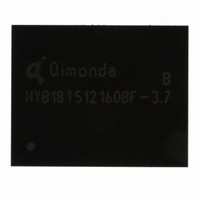
HYB18T1G160BF-5 Qimonda, HYB18T1G160BF-5 Datasheet - Page 43

HYB18T1G160BF-5
Manufacturer Part Number
HYB18T1G160BF-5
Description
IC DDR2 SDRAM 1GBIT 84TFBGA
Manufacturer
Qimonda
Datasheet
1.HYB18T1G800BF-3S.pdf
(74 pages)
Specifications of HYB18T1G160BF-5
Format - Memory
RAM
Memory Type
DDR2 SDRAM
Memory Size
1G (64M x 16)
Speed
200MHz
Interface
Parallel
Voltage - Supply
1.7 V ~ 1.9 V
Operating Temperature
0°C ~ 95°C
Package / Case
84-TFBGA
Lead Free Status / RoHS Status
Lead free / RoHS Compliant
Other names
675-1018-2
1)
2)
3)
4) Data Bus consists of DQ, DM, DQS, DQS, RDQS, RDQS, LDQS, LDQS, UDQS and UDQS.
5) Definitions for
6) Timing parameter minimum and maximum values for
7) A = Activate, RA = Read with Auto-Precharge, D=DESELECT
Rev. 1.3, 2007-07
03062006-ZNH8-HURV
Parameter
Self-Refresh Current
CKE ≤ 0.2 V; external clock off, CK and CK at 0 V; Other control and address inputs are floating,
Data bus inputs are floating.
Operating Bank Interleave Read Current
1. All banks interleaving reads,
2. Timing pattern:
DDR2-400-333: A0 RA0 A1 RA1 A2 RA2 A3 RA3 D D D (11 clocks)
DDR2-533-333: A0 RA0 D A1 RA1 D A2 RA2 D A3 RA3 D D D D (15 clocks)
DDR2-667-444: A0 RA0 D D A1 RA1 D D A2 RA2 D D A3 RA3 D D D D D (19 clocks)
DDR2-667-555: A0 RA0 D D A1 RA1 D D A2 RA2 D D A3 RA3 D D D D D D (20 clocks)
DDR2-800-555: A0 RA0 D D D A1 RA1 D D D A2 RA2 D D D A3 RA3 D D D D D(22 clocks)
DDR2-800-666: A0 RA0 D D D A1 RA1 D D D A2 RA2 D D D A3 RA3 D D D D D D(23 clocks)
Parameter
LOW
HIGH
STABLE
FLOATING
SWITCHING
V
I
I
t
Address bus inputs are stable during deselects; Data bus is switching.
DD
DD
RC
DDQ
specifications are tested after the device is properly initialized.
parameter are specified with ODT disabled.
=
= 1.8 V ± 0.1 V;
t
RC(IDD)
,
I
DD
t
RRD
Description
defined as
defined as
defined as inputs are stable at a HIGH or LOW level
defined as inputs are
defined as: Inputs are changing between high and low every other clock (once per two clocks) for address
and control signals, and inputs changing between high and low every other clock (once per clock) for DQ
signals not including mask or strobes
: see
=
V
t
Table 47
DD
RRD(IDD)
= 1.8 V ± 0.1 V
V
V
; tFAW = tFAW(IDD); CKE is HIGH, CS is HIGH between valid commands.
IN
IN
I
≤
≥
OUT
V
V
IL(ac).MAX
IH(ac).MIN
= 0 mA; BL = 4, CL = CL
V
REF
=
V
DDQ
I
DD
/ 2
current measurements are defined in
43
(IDD)
, AL =
t
RCD(IDD)
-1 ×
1-Gbit Double-Data-Rate-Two SDRAM
HY[B/I]18T1G[40/80/16]0B[C/F](L/V)
t
CK(IDD)
Chapter
;
t
CK
=
7.
t
CK(IDD)
Internet Data Sheet
,
Definition for
Symbol Note
I
I
TABLE 47
DD6
DD7
1)2)3)4)5)
6)
1)2)3)4)5)
6)7)
I
DD


