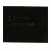
HYB18T1G160BF-5 Qimonda, HYB18T1G160BF-5 Datasheet - Page 5

HYB18T1G160BF-5
Manufacturer Part Number
HYB18T1G160BF-5
Description
IC DDR2 SDRAM 1GBIT 84TFBGA
Manufacturer
Qimonda
Datasheet
1.HYB18T1G800BF-3S.pdf
(74 pages)
Specifications of HYB18T1G160BF-5
Format - Memory
RAM
Memory Type
DDR2 SDRAM
Memory Size
1G (64M x 16)
Speed
200MHz
Interface
Parallel
Voltage - Supply
1.7 V ~ 1.9 V
Operating Temperature
0°C ~ 95°C
Package / Case
84-TFBGA
Lead Free Status / RoHS Status
Lead free / RoHS Compliant
Other names
675-1018-2
1.2
The 1-Gbit DDR2 DRAM is a high-speed Double-Data-Rate-
Two
1,073,741,824 bits and internally configured as anoctal
quadbank DRAM. The 1-Gbit device is organized as either
32 Mbit ×4 I/O ×8 banks, 16 Mbit ×8 I/O ×8 banks or 8 Mbit
×16 I/O ×8 banks chip. These devices achieve high speed
transfer rates starting at 400 Mb/sec/pin for general
applications.
The device is designed to comply with all DDR2 SDRAM key
features:
1. Posted CAS with additive latency,
2. Write latency = read latency - 1,
3. Normal and weak strength data-output driver,
4. Off-Chip Driver (OCD) impedance adjustment
5. On-Die Termination (ODT) function.
All of the control and address inputs are synchronized with a
pair of externally supplied differential clocks. Inputs are
Rev. 1.3, 2007-07
03062006-ZNH8-HURV
Product Type
Standard Temperature Range (0 °C - +70 °C)
HYB18T1G400BF-2.5F
HYB18T1G800BF-2.5F
HYB18T1G160BF-2.5F
HYB18T1G167BF-2.5F
HYB18T1G400BF-2.5
HYB18T1G800BF-2.5
HYB18T1G160BF-2.5
HYB18T1G167BF-2.5
HYB18T1G400BF-3
HYB18T1G800BF-3
HYB18T1G160BF-3
HYB18T1G167BF-3
HYB18T1G400BF-3S
HYB18T1G400BFL-3S
HYB18T1G800BF-3S
HYB18T1G800BFL-3S
HYB18T1G160BF-3S
HYB18T1G160BFL-3S
HYB18T1G160BFV-3S
HYB18T1G167BF-3S
CMOS
Synchronous
Description
Org. Speed
×4
×8
×16
×16
×4
×8
×16
×16
×4
×8
×16
×16
×4
×4
×8
×8
×16
×16
×16
×16
DRAM
DDR2-800D 5-5-5
DDR2-800E 6-6-6
DDR2-667C 4-4-4
DDR2-667D 5-5-5
device,
Ordering Information for Lead-Free Products (RoHS Compliant)
CAS-RCD-RP Latencies
containing
5
latched at the cross point of differential clocks (CK rising and
CK falling). All I/Os are synchronized with a single ended
DQS or differential DQS-DQS pair in a source synchronous
fashion.
A 17-bit address bus for ×4 and ×8 organised components
and a 16 bit address bus for ×16 components is used to
convey row, column and bank address information in a RAS-
CAS multiplexing style.
The DDR2 device operates with a 1.8 V
supply. An Auto-Refresh and Self-Refresh mode is provided
along with various power-saving power-down modes.
The functionality described and the timing specifications
included in this data sheet are for the DLL Enabled mode of
operation.
The DDR2 SDRAM is available in P(G)-TFBGA-68 and P(G)-
TFBGA-84 packages.
1)2)3)
Clock (MHz) Package
400
400
333
333
1-Gbit Double-Data-Rate-Two SDRAM
HY[B/I]18T1G[40/80/16]0B[C/F](L/V)
PG-TFBGA-68
PG-TFBGA-84
PG-TFBGA-92
PG-TFBGA-68
PG-TFBGA-84
PG-TFBGA-92
PG-TFBGA-68
PG-TFBGA-84
PG-TFBGA-92
PG-TFBGA-68
PG-TFBGA-84
PG-TFBGA-92
Internet Data Sheet
TABLE 5
±
0.1 V power
Note
4)


