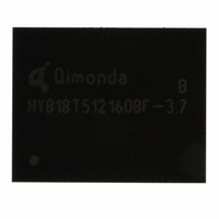
HYB18T1G160BF-5 Qimonda, HYB18T1G160BF-5 Datasheet - Page 42

HYB18T1G160BF-5
Manufacturer Part Number
HYB18T1G160BF-5
Description
IC DDR2 SDRAM 1GBIT 84TFBGA
Manufacturer
Qimonda
Datasheet
1.HYB18T1G800BF-3S.pdf
(74 pages)
Specifications of HYB18T1G160BF-5
Format - Memory
RAM
Memory Type
DDR2 SDRAM
Memory Size
1G (64M x 16)
Speed
200MHz
Interface
Parallel
Voltage - Supply
1.7 V ~ 1.9 V
Operating Temperature
0°C ~ 95°C
Package / Case
84-TFBGA
Lead Free Status / RoHS Status
Lead free / RoHS Compliant
Other names
675-1018-2
6
This chapter describes the current measurement specifications and conditions.
Rev. 1.3, 2007-07
03062006-ZNH8-HURV
Parameter
Operating Current - One bank Active - Precharge
t
Address and control inputs are switching; Databus inputs are switching.
Operating Current - One bank Active - Read - Precharge
I
CKE is HIGH, CS is HIGH between valid commands. Address and control inputs are switching; Databus
inputs are switching.
Precharge Power-Down Current
All banks idle; CKE is LOW;
floating
Precharge Standby Current
All banks idle; CS is HIGH; CKE is HIGH;
Data bus inputs are switching
Precharge Quiet Standby Current
All banks idle; CS is HIGH; CKE is HIGH;
Data bus inputs are floating.
Active Power-Down Current
All banks open;
are floating. MRS A12 bit is set to “0” (Fast Power-down Exit).
Active Power-Down Current
All banks open;
are floating. MRS A12 bit is set to 1 (Slow Power-down Exit);
Active Standby Current
All banks open;
commands. Address inputs are switching; Data Bus inputs are switching;
Operating Current
Burst Read: All banks open; Continuous burst reads; BL = 4; AL = 0, CL = CL
t
switching; Data Bus inputs are switching;
Operating Current
Burst Write: All banks open; Continuous burst writes; BL = 4; AL = 0, CL = CL
t
switching; Data Bus inputs are switching;
Burst Refresh Current
t
commands, Other control and address inputs are switching, Data bus inputs are switching.
Distributed Refresh Current
t
commands, Other control and address inputs are switching, Data bus inputs are switching.
CK
OUT
RAS
RAS
CK
CK
=
=
=
=
=
= 0 mA, BL = 4,
t
t
t
CK(IDD)
CK(IDD)
CK(IDD)
t
t
RAS.MAX.(IDD)
RAS.MAX(IDD)
.
,
, Refresh command every
, Refresh command every
t
RC
t
t
t
=
CK
CK
CK
,
,
t
t
t
RC(IDD)
=
=
=
RP
RP
Currents Measurement Conditions
t
t
t
t
CK
CK(IDD)
CK(IDD)
CK(IDD)
=
=
t
=
t
RP(IDD)
,
RP(IDD)
t
t
RAS
CK(IDD)
, CKE is LOW; Other control and address inputs are stable; Data bus inputs
, CKE is LOW; Other control and address inputs are stable, Data bus inputs
;
t
CK
t
.
RAS
; CKE is HIGH, CS is HIGH between valid commands. Address inputs are
=
; CKE is HIGH, CS is HIGH between valid commands. Address inputs are
=
t
,
t
RAS.MIN(IDD)
=
t
CK(IDD)
RC
t
RAS.MAX(IDD)
=
t
t
REFI
RFC
t
;Other control and address inputs are stable; Data bus inputs are
RC(IDD)
I
t
t
OUT
CK
CK
=
= 7.8 µs interval, CKE is LOW and CS is HIGH between valid
, CKE is HIGH, CS is HIGH between valid commands.
t
=
=
RFC(IDD)
,
= 0 mA.
,
t
t
t
CK(IDD)
CK(IDD)
RAS
t
RP
=
=
interval, CKE is HIGH, CS is HIGH between valid
t
; Other control and address inputs are switching,
; Other control and address inputs are stable,
t
RP(IDD)
RAS.MIN(IDD)
; CKE is HIGH, CS is HIGH between valid
42
,
t
RCD
=
t
RCD(IDD)
(IDD)
(IDD)
, AL = 0, CL = CL(IDD);
1-Gbit Double-Data-Rate-Two SDRAM
;
;
t
t
CK
CK
HY[B/I]18T1G[40/80/16]0B[C/F](L/V)
=
=
t
t
CK(IDD)
CK(IDD)
I
DD
Measurement Conditions
;
;
Internet Data Sheet
Symbol Note
I
I
I
I
I
I
I
I
I
I
I
I
TABLE 46
DD0
DD1
DD2P
DD2N
DD2Q
DD3P(0)
DD3P(1)
DD3N
DD4R
DD4W
DD5B
DD5D
1)2)3)4)5)
6)
1)2)3)4)5)
6)
1)2)3)4)5)
6)
1)2)3)4)5)
6)
1)2)3)4)5)
6)
1)2)3)4)5)
6)
1)2)3)4)5)
6)
1)2)3)4)5)
6)
1)2)3)4)5)
6)
1)2)3)4)5)
6)
1)2)3)4)5)
6)
1)2)3)4)5)
6)


