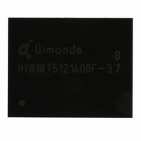
HYB18T1G160BF-5 Qimonda, HYB18T1G160BF-5 Datasheet - Page 58

HYB18T1G160BF-5
Manufacturer Part Number
HYB18T1G160BF-5
Description
IC DDR2 SDRAM 1GBIT 84TFBGA
Manufacturer
Qimonda
Datasheet
1.HYB18T1G800BF-3S.pdf
(74 pages)
Specifications of HYB18T1G160BF-5
Format - Memory
RAM
Memory Type
DDR2 SDRAM
Memory Size
1G (64M x 16)
Speed
200MHz
Interface
Parallel
Voltage - Supply
1.7 V ~ 1.9 V
Operating Temperature
0°C ~ 95°C
Package / Case
84-TFBGA
Lead Free Status / RoHS Status
Lead free / RoHS Compliant
Other names
675-1018-2
11) MIN (
12) The
13) The Auto-Refresh command interval has be reduced to 3.9 µs when operating the DDR2 DRAM in a temperature range between 85 °C
14) 0 °C≤
15) 85 °C <
16) A maximum of eight Auto-Refresh commands can be posted to any given DDR2 SDRAM device.
17) The
18) The maximum limit for the
19) Minimum
20) User can choose two different active power-down modes for additional power saving via MRS address bit A12. In “standard active power-
21) WR must be programmed to fulfill the minimum requirement for the
Rev. 1.3, 2007-07
03062006-ZNH8-HURV
Parameter
DQ output access time from CK / CK
CAS A to CAS B command period
CK, CK high-level width
CKE minimum high and low pulse width
CK, CK low-level width
Auto-Precharge write recovery + precharge
time
Minimum time clocks remain ON after CKE
asynchronously drops LOW
DQ and DM input hold time (differential data
strobe)
DQ and DM input hold time (single ended data
strobe)
DQ and DM input pulse width (each input)
DQS output access time from CK / CK
DQS input low (high) pulse width (write cycle)
DQS-DQ skew (for DQS & associated DQ
signals)
Write command to 1st DQS latching transition
DQ and DM input setup time (differential data
strobe)
be greater than the minimum specification limits for
(
parameters are verified by design and characterization, but not subject to production test.
and 95 °C.
Products (RoHS Compliant)” on Page
performance (bus turnaround) degrades accordingly.
down mode” (MR, A12 = “0”) a fast power-down exit timing
power-down exit timing
up to the next integer value.
refers to the application clock period. WR refers to the WR parameter stored in the MRS.
t
HZ,
t
t
t
HZ
RPST
RRD
t
CL
T
,
CASE
,
T
t
RPST
), or begins driving (
timing parameter depends on the page size of the DRAM organization. See
t
CASE
t
CH
WTR
) refers to the smaller of the actual clock low time and the actual clock high time as provided to the device (i.e. this value can
≤ 85 °C
and
≤ 95 °C
is two clocks when operating the DDR2-SDRAM at frequencies ≤ 200 ΜΗz.
t
LZ
,
t
RPRE
t
XARDS
t
parameters are referenced to a specific voltage level, which specify when the device output is no longer driving
WPST
t
t
DAL
LZ,
has to be satisfied.
t
parameter is not a device limit. The device operates with a greater value for this parameter, but system
= WR + (
RPRE
).
t
HZ
5.
t
RP
and
/
t
CK
t
DRAM Component Timing Parameter by Speed Grade - DDR2-400
LZ
). For each of the terms, if not already an integer, round to the next highest integer.
transitions occur in the same access time windows as valid data transitions.These
Symbol
t
t
t
t
t
t
t
t
t
t
t
t
t
t
t
AC
CCD
CH
CKE
CL
DAL
DELAY
DH
DH1
DIPW
DQSCK
DQSL,H
DQSQ
DQSS
DS
t
CL
(base)
(base)
and
(base)
t
t
CH
XARD
).
58
can be used. In “low active power-down mode” (MR, A12 =”1”) a slow
t
WR
DDR2–400
–600
2
0.45
3
0.45
WR +
t
275
–25
0.35
–500
0.35
—
– 0.25
150
Min.
IS
timing parameter, where
+
t
CK
t
RP
+
t
IH
Table 5 “Ordering Information for Lead-Free
1-Gbit Double-Data-Rate-Two SDRAM
HY[B/I]18T1G[40/80/16]0B[C/F](L/V)
Max.
+600
—
0.55
—
0.55
—
––
––
—
—
+500
—
350
+ 0.25
—
WR
MIN
[cycles] =
Unit
ps
t
t
t
t
t
ns
ps
ps
t
ps
t
ps
t
ps
Internet Data Sheet
CK
CK
CK
CK
CK
CK
CK
CK
t
WR
(ns)/
TABLE 56
t
CK
Note
6)
7)20)
8)
9)
10)
10)
10)
(ns) rounded
1)2)3)4)5)
t
CK


