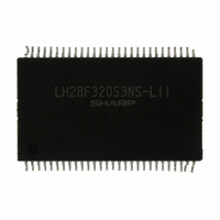
LH28F320S3NS-L11 Sharp Microelectronics, LH28F320S3NS-L11 Datasheet - Page 9

LH28F320S3NS-L11
Manufacturer Part Number
LH28F320S3NS-L11
Description
IC FLASH 32MBIT 110NS 56SSOP
Manufacturer
Sharp Microelectronics
Datasheet
1.LH28F320S3NS-L11.pdf
(62 pages)
Specifications of LH28F320S3NS-L11
Format - Memory
FLASH
Memory Type
FLASH
Memory Size
32M (4Mx8, 2Mx16)
Speed
110ns
Interface
Parallel
Voltage - Supply
3 V ~ 3.6 V
Operating Temperature
0°C ~ 70°C
Package / Case
56-SSOP
Lead Free Status / RoHS Status
Contains lead / Request inventory verification
Other names
425-1844
LHF32K01
LHF32K01
Available stocks
Company
Part Number
Manufacturer
Quantity
Price
Company:
Part Number:
LH28F320S3NS-L11
Manufacturer:
SHARP
Quantity:
5 380
Company:
Part Number:
LH28F320S3NS-L11
Manufacturer:
SHARP
Quantity:
5 380
Part Number:
LH28F320S3NS-L11
Manufacturer:
SHARP
Quantity:
20 000
sharp
2 PRINCIPLES OF OPERATION
The LH28F320S3NS-L11 Flash memory includes an
on-chip WSM to manage block erase, full chip erase,
(multi)
configuration functions. It allows for: 100% TTL-level
control inputs, fixed power supplies during block
erase, full chip erase, (multi) word/byte write and
block lock-bit configuration, and minimal processor
overhead with RAM-Like interface timings.
After initial device power-up or return from deep
power-down mode (see Bus Operations), the device
defaults to read array mode. Manipulation of external
memory control pins allow array read, standby, and
output disable operations.
Status register, query structure and identifier codes
can be accessed through the CUI independent of the
V
block erase, full chip erase, (multi) word/byte write
and
associated with altering memory contentsblock
erase, full chip erase, (multi) word/byte write and
block
identifier codesare accessed via the CUI and
verified through the status register.
Commands
microprocessor write timings. The CUI contents serve
as input to the WSM, which controls the block erase,
full chip erase, (multi) word/byte write and block lock-
bit
regulated by the WSM, including pulse repetition,
internal
Addresses and data are internally latch during write
cycles. Writing the appropriate command outputs
array data, accesses the identifier codes, outputs
query structure or outputs status register data.
PP
voltage. High voltage on V
configuration.
block
lock-bit configuration, status, query and
word/byte
verification,
lock-bit
are
The
write
configuration.
written
and
internal
and
margining
PP
enables successful
using
algorithms
block
All
of
functions
standard
lock-bit
data.
are
LHF32K01
Interface software that initiates and polls progress of
block erase, full chip erase, (multi) word/byte write
and block lock-bit configuration can be stored in any
block. This code is copied to and executed from
system RAM during flash memory updates. After
successful completion, reads are again possible via
the Read Array command. Block erase suspend
allows system software to suspend a block erase to
read or write data from any other block. Write
suspend allows system software to suspend a (multi)
word/byte write to read data from any other flash
memory array location.
2.1 Data Protection
Depending on the application, the system designer
may choose to make the V
switchable (available only when block erase, full chip
erase, (multi) word/byte write and block lock-bit
configuration are required) or hardwired to V
The device accommodates either design practice and
encourages optimization of the processor-memory
interface.
When V
altered. The CUI, with multi-step block erase, full chip
erase, (multi) word/byte write and block lock-bit
configuration
protection from unwanted operations even when high
voltage is applied to V
disabled when V
V
locking capability provides additional protection from
inadvertent code or data alteration by gating block
erase, full chip erase and (multi) word/byte write
operations.
LKO
or when RP# is at V
PP
≤V
PPLK
command
CC
, memory contents cannot be
is below the write lockout voltage
PP
. All write functions are
sequences,
IL
. The device’s block
PP
power supply
Rev. 1.55
provides
PPH1/2/3
6
.


