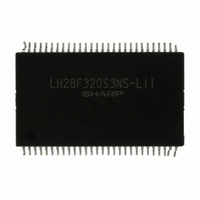
LH28F320S3NS-L11 Sharp Microelectronics, LH28F320S3NS-L11 Datasheet - Page 18

LH28F320S3NS-L11
Manufacturer Part Number
LH28F320S3NS-L11
Description
IC FLASH 32MBIT 110NS 56SSOP
Manufacturer
Sharp Microelectronics
Datasheet
1.LH28F320S3NS-L11.pdf
(62 pages)
Specifications of LH28F320S3NS-L11
Format - Memory
FLASH
Memory Type
FLASH
Memory Size
32M (4Mx8, 2Mx16)
Speed
110ns
Interface
Parallel
Voltage - Supply
3 V ~ 3.6 V
Operating Temperature
0°C ~ 70°C
Package / Case
56-SSOP
Lead Free Status / RoHS Status
Contains lead / Request inventory verification
Other names
425-1844
LHF32K01
LHF32K01
Available stocks
Company
Part Number
Manufacturer
Quantity
Price
Company:
Part Number:
LH28F320S3NS-L11
Manufacturer:
SHARP
Quantity:
5 380
Company:
Part Number:
LH28F320S3NS-L11
Manufacturer:
SHARP
Quantity:
5 380
Part Number:
LH28F320S3NS-L11
Manufacturer:
SHARP
Quantity:
20 000
sharp
4.5.4 Device Geometry Definition
This field provides critical details of the flash device geometry.
4.5.5 SCS OEM Specific Extended Query Table
Certain flash features and commands may be optional in a vendor-specific algorithm specification. The optional
vendor-specific Query table(s) may be used to specify this and other types of information. These structures are
defined solely by the flash vendor(s).
27H
28H,29H
2AH,2BH
2CH
2DH,2EH
2FH,30H
31H,32H,33H
34H
35H
36H,37H,
38H,39H
3AH
3BH,3CH
3DH
3EH
3FH
(Word Address)
(Word Address)
Offset
Offset
reserved Reserved for future versions of the SCS Specification
Length
Length
01H
02H
02H
01H
02H
02H
03H
01H
01H
04H
01H
02H
01H
01H
Table 11. SCS OEM Specific Extended Query Table
Device Size
16H (16H=22, 2
Flash Device Interface description
02H,00H (x8/x16 supports x8 and x16 via BYTE#)
Maximum Number of Bytes in Multi-byte
05H,00H (2
Number of Erase Block Regions within device
01H (symmetrically blocked)
The Number of Erase Blocks
3FH,00H (3FH=63 ==> 63+1=64 Blocks)
The Number of "256 Bytes" cluster in a Erase block
00H,01H (0100H=256 ==>256 Bytes x 256= 64K Bytes in a Erase Block)
PRI
50H,52H,49H
31H (1) Major Version Number , ASCII
30H (0) Minor Version Number, ASCII
0FH,00H,00H,00H
Optional Command Support
01H
Supported Functions after Suspend
03H,00H
Block Status Register Mask
V
33H(3.3V)
V
50H(5.0V)
CC
PP
Table 10. Device Geometry Definition
Programming Supply Optimum Write/Erase voltage(highest performance)
Logic Supply Optimum Write/Erase voltage(highest performance)
bit0=1 : Chip Erase Supported
bit1=1 : Suspend Erase Supported
bit2=1 : Suspend Write Supported
bit3=1 : Lock/Unlock Supported
bit4=0 : Queued Erase Not Supported
bit5-31=0 : reserved for future use
bit0=1 : Write Supported after Erase Suspend
bit1-7=0 : reserved for future use
bit0=1 : Block Status Register Lock Bit [BSR.0] active
bit1=1 : Block Status Register Valid Bit [BSR.1] active
bit2-15=0 : reserved for future use
5
=32 Bytes )
22
LHF32K01
=4194304=4M Bytes)
Description
Description
Rev. 1.55
15


