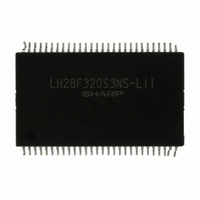
LH28F320S3NS-L11 Sharp Microelectronics, LH28F320S3NS-L11 Datasheet - Page 6

LH28F320S3NS-L11
Manufacturer Part Number
LH28F320S3NS-L11
Description
IC FLASH 32MBIT 110NS 56SSOP
Manufacturer
Sharp Microelectronics
Datasheet
1.LH28F320S3NS-L11.pdf
(62 pages)
Specifications of LH28F320S3NS-L11
Format - Memory
FLASH
Memory Type
FLASH
Memory Size
32M (4Mx8, 2Mx16)
Speed
110ns
Interface
Parallel
Voltage - Supply
3 V ~ 3.6 V
Operating Temperature
0°C ~ 70°C
Package / Case
56-SSOP
Lead Free Status / RoHS Status
Contains lead / Request inventory verification
Other names
425-1844
LHF32K01
LHF32K01
Available stocks
Company
Part Number
Manufacturer
Quantity
Price
Company:
Part Number:
LH28F320S3NS-L11
Manufacturer:
SHARP
Quantity:
5 380
Company:
Part Number:
LH28F320S3NS-L11
Manufacturer:
SHARP
Quantity:
5 380
Part Number:
LH28F320S3NS-L11
Manufacturer:
SHARP
Quantity:
20 000
sharp
1 INTRODUCTION
This
specifications. Section 1 provides a flash memory
overview. Sections 2, 3, 4, and 5 describe the
memory organization and functionality. Section 6
covers electrical specifications.
1.1 Product Overview
The LH28F320S3NS-L11 is a high-performance 32-
Mbit
4MBx8/2MBx16. The 4MB of data is arranged in
sixty-four 64-Kbyte blocks which are individually
erasable, lockable, and unlockable in-system. The
memory map is shown in Figure 3.
Smart 3 technology provides a choice of V
V
system performance and power expectations. 2.7V
V
5V V
a separate 12V converter. In addition to flexible erase
and program voltages, the dedicated V
complete data protection when V
Internal
automatically configures the device for optimized
read and write operations.
A Command User Interface (CUI) serves as the
interface between the system processor and internal
operation of the device. A valid command sequence
written to the CUI initiates device automation. An
internal Write State Machine (WSM) automatically
executes the algorithms and timings necessary for
block erase, full chip erase, (multi) word/byte write
and block lock-bit configuration operations.
A block erase operation erases one of the device’s
64-Kbyte blocks typically within 0.41s (3.3V V
V
independently erased 100,000 times (6.4 million
block erases per device). Block erase suspend mode
allows system software to suspend block erase to
read or write data from any other block.
A word/byte write is performed in byte increments
typically within 12.95µs (3.3V V
word/byte write has high speed write performance of
2.7µs/byte (3.3V V
write suspend mode enables the system to read data
PP
CC
PP
Table 1. V
) independent of other blocks. Each block can be
CC
consumes approximately one-fifth the power of
combinations, as shown in Table 1, to meet
Smart
V
. V
datasheet
CC
Offered by Smart 3 Technology
PP
V
2.7V
3.3V
Voltage
CC
at 2.7V and 3.3V eliminates the need for
CC
3
and V
and
Flash
CC
contains
, 5V V
PP
V
Voltage Combinations
PP
memory
PP
CC
LH28F320S3NS-L11
PP
2.7V, 3.3V, 5V
detection
). (Multi) Word/byte
V
, 5V V
PP
≤ V
3.3V, 5V
Voltage
organized
PPLK
PP
PP
.
). A multi
pin gives
Circuitry
CC
CC
, 5V
and
LHF32K01
as
or execute code from any other flash memory array
location.
Individual block locking uses a combination of bits
and WP#, Sixty-four block lock-bits, to lock and
unlock blocks. Block lock-bits gate block erase, full
chip erase and (multi) word/byte write operations.
Block lock-bit configuration operations (Set Block
Lock-Bit and Clear Block Lock-Bits commands) set
and cleared block lock-bits.
The status register indicates when the WSM’s block
erase, full chip erase, (multi) word/byte write or block
lock-bit configuration operation is finished.
The STS output gives an additional indicator of WSM
activity by providing both a hardware signal of status
(versus
(interrupt masking for background block erase, for
example). Status polling using STS minimizes both
CPU overhead and system power consumption. STS
pin can be configured to different states using the
Configuration command. The STS pin defaults to
RY/BY# operation. When low, STS indicates that the
WSM is performing a block erase, full chip erase,
(multi) word/byte write or block lock-bit configuration.
STS-High Z indicates that the WSM is ready for a
new command, block erase is suspended and (multi)
word/byte write are inactive, (multi) word/byte write
are suspended, or the device is in deep power-down
mode. The other 3 alternate configurations are all
pulse mode for use as a system interrupt.
The access time is 110ns (t
commercial temperature range (0°C to +70°C) and
V
voltage, the access time is 140ns (2.7V-3.6V).
The
substantially reduces active current when the device
is in static mode (addresses not switching). In APS
mode, the typical I
When either CE
the I
RP# pin is at GND, deep power-down mode is
enabled which minimizes power consumption and
provides write protection during reset. A reset time
(t
outputs are valid. Likewise, the device has a wake
time (t
recognized. With RP# at GND, the WSM is reset and
the status register is cleared.
The device is available in 56-Lead SSOP (Shrink
Small Outline Package). Pinout is shown in Figure 2.
PHQV
CC
CC
supply voltage range of 3.0V-3.6V. At lower V
Automatic
) is required from RP# switching high until
PHEL
CMOS standby mode is enabled. When the
software
) from RP#-high until writes to the CUI are
0
# or CE
CCR
Power
polling)
current is 3 mA at 3.3V V
1
#, and RP# pins are at V
Savings
and
AVQV
status
(APS)
) over the
Rev. 1.55
masking
feature
CC
CC
.
CC
3
,


