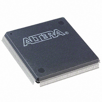
EP3C16Q240C8N Altera, EP3C16Q240C8N Datasheet - Page 87

EP3C16Q240C8N
Manufacturer Part Number
EP3C16Q240C8N
Description
IC CYCLONE III FPGA 16K 240PQFP
Manufacturer
Altera
Series
Cyclone® IIIr
Datasheets
1.EP3C5F256C8N.pdf
(5 pages)
2.EP3C5F256C8N.pdf
(34 pages)
3.EP3C5F256C8N.pdf
(66 pages)
4.EP3C5F256C8N.pdf
(14 pages)
5.EP3C5F256C8N.pdf
(76 pages)
6.EP3C16Q240C8N.pdf
(274 pages)
Specifications of EP3C16Q240C8N
Number Of Logic Elements/cells
15408
Number Of Labs/clbs
963
Total Ram Bits
516096
Number Of I /o
160
Voltage - Supply
1.15 V ~ 1.25 V
Mounting Type
Surface Mount
Operating Temperature
0°C ~ 85°C
Package / Case
240-MQFP, 240-PQFP
Family Name
Cyclone III
Number Of Logic Blocks/elements
15408
# I/os (max)
92
Frequency (max)
402MHz
Process Technology
65nm
Operating Supply Voltage (typ)
1.2V
Logic Cells
15408
Ram Bits
516096
Operating Supply Voltage (min)
1.15V
Operating Supply Voltage (max)
1.25V
Operating Temp Range
0C to 85C
Operating Temperature Classification
Commercial
Mounting
Surface Mount
Pin Count
240
Package Type
PQFP
For Use With
544-2601 - KIT DEV CYCLONE III LS EP3CLS200P0037 - BOARD DEV/EDUCATION ALTERA DE0544-2411 - KIT DEV NIOS II CYCLONE III ED.
Lead Free Status / RoHS Status
Lead free / RoHS Compliant
Number Of Gates
-
Lead Free Status / Rohs Status
Compliant
Other names
544-2458
Available stocks
Company
Part Number
Manufacturer
Quantity
Price
Company:
Part Number:
EP3C16Q240C8N
Manufacturer:
ALTERA64
Quantity:
74
Chapter 5: Clock Networks and PLLs in the Cyclone III Device Family
Phase Shift Implementation
Figure 5–18. Delay Insertion Using VCO Phase Output and Counter Delay Time
© December 2009
CLK0
CLK1
CLK2
135
180
225
270
315
45
90
0
1/8 t
VCO
Altera Corporation
Coarse resolution phase shifts are implemented by delaying the start of the counters
for a predetermined number of counter clocks.
shift.
Equation 5–2. Coarse Resolution Phase Shift
C is the count value set for the counter delay time (this is the initial setting in the PLL
usage section of the compilation report in the Quartus II software). If the initial value
is 1, C – 1 = 0° phase shift.
Figure 5–18
VCO phase taps method. The eight phases from the VCO are shown and labeled for
reference. In this example, CLK0 is based on 0
value for the counter set to one. The CLK1 signal is divided by four, two VCO clocks
for high time and two VCO clocks for low time. CLK1 is based on the 135° phase tap
from the VCO and has the C value for the counter set to one. The CLK1 signal is also
divided by four. In this case, the two clocks are offset by 3 Φ
0° phase from the VCO but has the C value for the counter set to three. This creates a
delay of two Φ
You can use the coarse and fine phase shifts to implement clock delays in the
Cyclone III device family.
The Cyclone III device family supports dynamic phase shifting of VCO phase taps
only. The phase shift is configurable for any number of times. Each phase shift takes
about one scanclk cycle, allowing you to implement large phase shifts quickly.
Φ coarse
t
d0-1
=
t
d0-2
C 1
----------- -
f
VCO
–
shows an example of phase shift insertion using fine resolution through
coarse
t
=
VCO
(
-------------------- -
C 1
(two complete VCO periods).
Mf
–
R EF
) N
°
phase from the VCO and has the C
Equation 5–2
Cyclone III Device Handbook, Volume 1
fine
shows the coarse phase
. CLK2 is based on the
5–23


