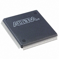
EP3C16Q240C8N Altera, EP3C16Q240C8N Datasheet - Page 151

EP3C16Q240C8N
Manufacturer Part Number
EP3C16Q240C8N
Description
IC CYCLONE III FPGA 16K 240PQFP
Manufacturer
Altera
Series
Cyclone® IIIr
Datasheets
1.EP3C5F256C8N.pdf
(5 pages)
2.EP3C5F256C8N.pdf
(34 pages)
3.EP3C5F256C8N.pdf
(66 pages)
4.EP3C5F256C8N.pdf
(14 pages)
5.EP3C5F256C8N.pdf
(76 pages)
6.EP3C16Q240C8N.pdf
(274 pages)
Specifications of EP3C16Q240C8N
Number Of Logic Elements/cells
15408
Number Of Labs/clbs
963
Total Ram Bits
516096
Number Of I /o
160
Voltage - Supply
1.15 V ~ 1.25 V
Mounting Type
Surface Mount
Operating Temperature
0°C ~ 85°C
Package / Case
240-MQFP, 240-PQFP
Family Name
Cyclone III
Number Of Logic Blocks/elements
15408
# I/os (max)
92
Frequency (max)
402MHz
Process Technology
65nm
Operating Supply Voltage (typ)
1.2V
Logic Cells
15408
Ram Bits
516096
Operating Supply Voltage (min)
1.15V
Operating Supply Voltage (max)
1.25V
Operating Temp Range
0C to 85C
Operating Temperature Classification
Commercial
Mounting
Surface Mount
Pin Count
240
Package Type
PQFP
For Use With
544-2601 - KIT DEV CYCLONE III LS EP3CLS200P0037 - BOARD DEV/EDUCATION ALTERA DE0544-2411 - KIT DEV NIOS II CYCLONE III ED.
Lead Free Status / RoHS Status
Lead free / RoHS Compliant
Number Of Gates
-
Lead Free Status / Rohs Status
Compliant
Other names
544-2458
Available stocks
Company
Part Number
Manufacturer
Quantity
Price
Company:
Part Number:
EP3C16Q240C8N
Manufacturer:
ALTERA64
Quantity:
74
Chapter 8: External Memory Interfaces in the Cyclone III Device Family
Cyclone III Device Family Memory Interfaces Pin Support
Table 8–2. Cyclone III LS Device DQS and DQ Bus Mode Support for Each Side of the Device
© January 2010 Altera Corporation
EP3CLS100
EP3CLS150
EP3CLS200
Notes to
(1) These numbers are preliminary until characterization is completed.
(2) This device package does not support x32 or 36 mode.
Device
Table
f
8–2:
484-pin FineLine
BGA/
484-pin Ultra FineLine
BGA
780-pin FineLine BGA
484-pin FineLine BGA
(2)
780-pin FineLine BGA
484-pin FineLine BGA
(2)
780-pin FineLine BGA
(2)
For more information about device package outline, refer to the
Specifications
DQS pins are listed in the Cyclone III and Cyclone III LS pin tables as DQSXY, in which
X indicates the DQS grouping number and Y indicates whether the group is located on
the top (T), bottom (B), left (L) or right (R) side of the device. Similarly, the
corresponding DQ pins are marked as DQXY, in which the X denotes the DQ grouping
number and Y denotes whether the group is located on the top (T), bottom (B), left (L)
or right (R) side of the device. For example, DQS2T indicates a DQS pin belonging to
group 2, located on the top side of the device. Similarly, the DQ pins belonging to that
group is shown as DQ2T.
Package
page.
Bottom
Bottom
Bottom
Bottom
Bottom
Bottom
Right
Right
Right
Right
Right
Right
Side
Left
Left
Left
Left
Left
Left
Top
Top
Top
Top
Top
Top
Number
Groups
of ×8
2
2
2
2
4
4
6
6
2
2
2
2
4
4
6
6
2
2
2
2
4
4
6
6
Number
Groups
of ×9
2
2
2
2
2
2
2
2
2
2
2
2
2
2
2
2
2
2
2
2
2
2
2
2
Number
Groups
of ×16
1
1
1
1
2
2
2
2
1
1
1
1
2
2
2
2
1
1
1
1
2
2
2
2
Cyclone III Device Handbook, Volume 1
Number
Groups
of ×18
(Note 1)
1
1
1
1
2
2
2
2
1
1
1
1
2
2
2
2
1
1
1
1
2
2
2
2
Device Packaging
Number
Groups
of ×32
(Part 2 of 2)
—
—
—
—
—
—
—
—
—
—
—
—
1
1
1
1
1
1
1
1
1
1
1
1
Number
Groups
of ×36
—
—
—
—
—
—
—
—
—
—
—
—
1
1
1
1
1
1
1
1
1
1
1
1
8–7


