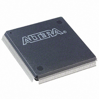
EP3C16Q240C8N Altera, EP3C16Q240C8N Datasheet - Page 41

EP3C16Q240C8N
Manufacturer Part Number
EP3C16Q240C8N
Description
IC CYCLONE III FPGA 16K 240PQFP
Manufacturer
Altera
Series
Cyclone® IIIr
Datasheets
1.EP3C5F256C8N.pdf
(5 pages)
2.EP3C5F256C8N.pdf
(34 pages)
3.EP3C5F256C8N.pdf
(66 pages)
4.EP3C5F256C8N.pdf
(14 pages)
5.EP3C5F256C8N.pdf
(76 pages)
6.EP3C16Q240C8N.pdf
(274 pages)
Specifications of EP3C16Q240C8N
Number Of Logic Elements/cells
15408
Number Of Labs/clbs
963
Total Ram Bits
516096
Number Of I /o
160
Voltage - Supply
1.15 V ~ 1.25 V
Mounting Type
Surface Mount
Operating Temperature
0°C ~ 85°C
Package / Case
240-MQFP, 240-PQFP
Family Name
Cyclone III
Number Of Logic Blocks/elements
15408
# I/os (max)
92
Frequency (max)
402MHz
Process Technology
65nm
Operating Supply Voltage (typ)
1.2V
Logic Cells
15408
Ram Bits
516096
Operating Supply Voltage (min)
1.15V
Operating Supply Voltage (max)
1.25V
Operating Temp Range
0C to 85C
Operating Temperature Classification
Commercial
Mounting
Surface Mount
Pin Count
240
Package Type
PQFP
For Use With
544-2601 - KIT DEV CYCLONE III LS EP3CLS200P0037 - BOARD DEV/EDUCATION ALTERA DE0544-2411 - KIT DEV NIOS II CYCLONE III ED.
Lead Free Status / RoHS Status
Lead free / RoHS Compliant
Number Of Gates
-
Lead Free Status / Rohs Status
Compliant
Other names
544-2458
Available stocks
Company
Part Number
Manufacturer
Quantity
Price
Company:
Part Number:
EP3C16Q240C8N
Manufacturer:
ALTERA64
Quantity:
74
Chapter 3: Memory Blocks in the Cyclone III Device Family
Overview
Packed Mode Support
Address Clock Enable Support
© December 2009
Altera Corporation
Figure 3–2
Figure 3–2. Cyclone III Device Family byteena Functional Waveform
Note to
(1) For this functional waveform, New Data mode is selected.
When a byteena bit is deasserted during a write cycle, the old data in the memory
appears in the corresponding data-byte output. When a byteena bit is asserted
during a write cycle, the corresponding data-byte output depends on the setting
chosen in the Quartus
the old data at that location.
Cyclone III device family M9K memory blocks support packed mode. You can
implement two single-port memory blocks in a single block under the following
conditions:
■
■
Cyclone III device family M9K memory blocks support an active-low address clock
enable, which holds the previous address value for as long as the addressstall
signal is high (addressstall = '1'). When you configure M9K memory blocks in
dual-port mode, each port has its own independent address clock enable.
contents at a0
contents at a1
contents at a2
Each of the two independent block sizes is less than or equal to half of the M9K
block size. The maximum data width for each independent block is 18 bits wide.
Each of the single-port memory blocks is configured in single-clock mode. For
more information about packed mode support, refer to
page 3–8
q (asynch)
address
byteena
Figure
inclock
wren
rden
data
shows how the wren and byteena signals control the RAM operations.
3–2:
and
XXXX
XX
an
FFFF
“Single-Clock Mode” on page
doutn
FFFF
®
II software. The setting can either be the newly written data or
10
a0
FFFF
ABFF
ABCD
01
a1
FFCD
11
a2
3–16.
ABCD
ABFF
a0
FFCD
Cyclone III Device Handbook, Volume 1
ABFF
“Single-Port Mode” on
(Note 1)
ABCD
a1
XXXX
XX
FFCD
a2
ABCD
3–5


