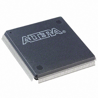
EP3C16Q240C8N Altera, EP3C16Q240C8N Datasheet - Page 193

EP3C16Q240C8N
Manufacturer Part Number
EP3C16Q240C8N
Description
IC CYCLONE III FPGA 16K 240PQFP
Manufacturer
Altera
Series
Cyclone® IIIr
Datasheets
1.EP3C5F256C8N.pdf
(5 pages)
2.EP3C5F256C8N.pdf
(34 pages)
3.EP3C5F256C8N.pdf
(66 pages)
4.EP3C5F256C8N.pdf
(14 pages)
5.EP3C5F256C8N.pdf
(76 pages)
6.EP3C16Q240C8N.pdf
(274 pages)
Specifications of EP3C16Q240C8N
Number Of Logic Elements/cells
15408
Number Of Labs/clbs
963
Total Ram Bits
516096
Number Of I /o
160
Voltage - Supply
1.15 V ~ 1.25 V
Mounting Type
Surface Mount
Operating Temperature
0°C ~ 85°C
Package / Case
240-MQFP, 240-PQFP
Family Name
Cyclone III
Number Of Logic Blocks/elements
15408
# I/os (max)
92
Frequency (max)
402MHz
Process Technology
65nm
Operating Supply Voltage (typ)
1.2V
Logic Cells
15408
Ram Bits
516096
Operating Supply Voltage (min)
1.15V
Operating Supply Voltage (max)
1.25V
Operating Temp Range
0C to 85C
Operating Temperature Classification
Commercial
Mounting
Surface Mount
Pin Count
240
Package Type
PQFP
For Use With
544-2601 - KIT DEV CYCLONE III LS EP3CLS200P0037 - BOARD DEV/EDUCATION ALTERA DE0544-2411 - KIT DEV NIOS II CYCLONE III ED.
Lead Free Status / RoHS Status
Lead free / RoHS Compliant
Number Of Gates
-
Lead Free Status / Rohs Status
Compliant
Other names
544-2458
Available stocks
Company
Part Number
Manufacturer
Quantity
Price
Company:
Part Number:
EP3C16Q240C8N
Manufacturer:
ALTERA64
Quantity:
74
Chapter 9: Configuration, Design Security, and Remote System Upgrades in the Cyclone III Device Family
Configuration Features
© December 2009
f
1
Altera Corporation
Programming Parallel Flash Memories
Supported parallel flash memories are external non-volatile configuration devices.
They are industry standard microprocessor flash memories. For more information
about the supported families for the commodity parallel flash, refer to
page
Cyclone III devices in a single- or multiple-device chains support in-system parallel
flash programming with the JTAG interface using the flash loader megafunction. For
Cyclone III devices, the board-intelligent host or download cable uses four JTAG pins
to program the parallel flash in system, even if the host or download cable cannot
access the configuration pins of the parallel flash.
For more information about using the JTAG pins on Cyclone III devices to program
the parallel flash in-system, refer to
(PFL) with the Quartus II
In the AP configuration scheme, the default configuration boot address is 0×010000
when represented in 16-bit word addressing in the supported parallel flash memory
(Figure
0x020000 because it is represented in 8-bit byte addressing. Cyclone III devices
configure from word address 0x010000, which is equivalent to byte address 0x020000.
The Quartus II software uses byte addressing for the default configuration boot
address. You must set the start address field to 0x020000.
The default configuration boot addressing allows the system to use special parameter
blocks in the flash memory map. Parameter blocks are at the top or bottom of the
memory map. The configuration boot address in the AP configuration scheme is
shown in
0x010000 to any desired address using the APFC_BOOT_ADDR JTAG instruction. For
more information about the APFC_BOOT_ADDR JTAG instruction, refer to
Instructions” on page
9–24.
9–13). In the Quartus II software, the default configuration boot address is
Figure
9–13. You can change the default configuration default boot address
9–61.
Software.
AN 478: Using FPGA-Based Parallel Flash Loader
Cyclone III Device Handbook, Volume 1
Table 9–11 on
“JTAG
9–33


