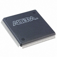
EP3C16Q240C8N Altera, EP3C16Q240C8N Datasheet - Page 113

EP3C16Q240C8N
Manufacturer Part Number
EP3C16Q240C8N
Description
IC CYCLONE III FPGA 16K 240PQFP
Manufacturer
Altera
Series
Cyclone® IIIr
Datasheets
1.EP3C5F256C8N.pdf
(5 pages)
2.EP3C5F256C8N.pdf
(34 pages)
3.EP3C5F256C8N.pdf
(66 pages)
4.EP3C5F256C8N.pdf
(14 pages)
5.EP3C5F256C8N.pdf
(76 pages)
6.EP3C16Q240C8N.pdf
(274 pages)
Specifications of EP3C16Q240C8N
Number Of Logic Elements/cells
15408
Number Of Labs/clbs
963
Total Ram Bits
516096
Number Of I /o
160
Voltage - Supply
1.15 V ~ 1.25 V
Mounting Type
Surface Mount
Operating Temperature
0°C ~ 85°C
Package / Case
240-MQFP, 240-PQFP
Family Name
Cyclone III
Number Of Logic Blocks/elements
15408
# I/os (max)
92
Frequency (max)
402MHz
Process Technology
65nm
Operating Supply Voltage (typ)
1.2V
Logic Cells
15408
Ram Bits
516096
Operating Supply Voltage (min)
1.15V
Operating Supply Voltage (max)
1.25V
Operating Temp Range
0C to 85C
Operating Temperature Classification
Commercial
Mounting
Surface Mount
Pin Count
240
Package Type
PQFP
For Use With
544-2601 - KIT DEV CYCLONE III LS EP3CLS200P0037 - BOARD DEV/EDUCATION ALTERA DE0544-2411 - KIT DEV NIOS II CYCLONE III ED.
Lead Free Status / RoHS Status
Lead free / RoHS Compliant
Number Of Gates
-
Lead Free Status / Rohs Status
Compliant
Other names
544-2458
Available stocks
Company
Part Number
Manufacturer
Quantity
Price
Company:
Part Number:
EP3C16Q240C8N
Manufacturer:
ALTERA64
Quantity:
74
Chapter 6: I/O Features in the Cyclone III Device Family
Termination Scheme for I/O Standards
Table 6–4. Cyclone III Device Family Supported I/O Standards and Constraints (Part 2 of 2)
Termination Scheme for I/O Standards
Voltage-Referenced I/O Standard Termination
© December 2009
RSDS and
mini-LVDS
BLVDS
LVPECL
Notes to
(1) The PCI-clamp diode must be enabled for 3.3-V/3.0-V LVTTL/LVCMOS.
(2) Differential HSTL and SSTL outputs use two single-ended outputs with the second output programmed as inverted. Differential HSTL and SSTL
(3) PPDS, mini-LVDS, and RSDS are only supported on output pins.
(4) LVPECL is only supported on clock inputs.
(5) Bus LVDS (BLVDS) output uses two single-ended outputs with the second output programmed as inverted. BLVDS input uses LVDS input buffer.
(6) Class I and Class II refer to output termination and do not apply to input. 1.2-V HSTL input is supported at both column and row I/O regardless of
(7) True differential LVDS, RSDS, and mini-LVDS I/O standards are supported in left and right I/O pins while emulated differential LVDS, RSDS, and
I/O Standard
inputs treat differential inputs as two single-ended HSTL and SSTL inputs and only decode one of them. Differential HSTL and SSTL are only
supported on CLK pins.
class.
mini-LVDS I/O standards are supported in both left and right, and top and bottom I/O pins.
(5)
Table
(4)
(3)
6–4:
Altera Corporation
Differential
Differential
Differential
The Cyclone III device family supports PCI and PCI-X I/O standards at 3.0-V V
The 3.0-V PCI and PCI-X I/O are fully compatible for direct interfacing with 3.3-V PCI
systems without requiring any additional components. The 3.0-V PCI and PCI-X
outputs meet the V
sufficient noise margin.
This section describes recommended termination schemes for voltage-referenced and
differential I/O standards.
The 3.3-V LVTTL, 3.0-V LVTTL and LVCMOS, 2.5-V LVTTL and LVCMOS, 1.8-V
LVTTL and LVCMOS, 1.5-V LVCMOS, 1.2-V LVCMOS, 3.0-V PCI, and PCI-X
I/O standards do not specify a recommended termination scheme per the JEDEC
standard
Voltage-referenced I/O standards require an input reference voltage (V
termination voltage (V
termination voltage of the transmitting device, as shown in
Type
Standard
Support
—
—
—
IH
and V
TT
). The reference voltage of the receiving device tracks the
IL
Input
requirements of 3.3-V PCI and PCI-X inputs with
2.5
2.5
V
—
C CIO
Level (in V)
Output
2.5
2.5
—
CLK,
DQS
Top and Bottom I/O Pins
—
—
v
PLL_OUT
Cyclone III Device Handbook, Volume 1
v
—
—
Figure 6–6
User
Pins
I/O
v
v
—
and
REF
) and a
Figure
CLK,
Left and Right
DQS
v
—
—
I/O Pins
CCIO
User I/O
6–7.
6–13
.
Pins
v
v
—


