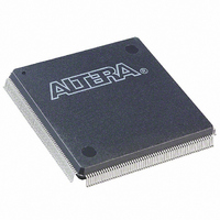
EP3C16Q240C8N Altera, EP3C16Q240C8N Datasheet - Page 35

EP3C16Q240C8N
Manufacturer Part Number
EP3C16Q240C8N
Description
IC CYCLONE III FPGA 16K 240PQFP
Manufacturer
Altera
Series
Cyclone® IIIr
Datasheets
1.EP3C5F256C8N.pdf
(5 pages)
2.EP3C5F256C8N.pdf
(34 pages)
3.EP3C5F256C8N.pdf
(66 pages)
4.EP3C5F256C8N.pdf
(14 pages)
5.EP3C5F256C8N.pdf
(76 pages)
6.EP3C16Q240C8N.pdf
(274 pages)
Specifications of EP3C16Q240C8N
Number Of Logic Elements/cells
15408
Number Of Labs/clbs
963
Total Ram Bits
516096
Number Of I /o
160
Voltage - Supply
1.15 V ~ 1.25 V
Mounting Type
Surface Mount
Operating Temperature
0°C ~ 85°C
Package / Case
240-MQFP, 240-PQFP
Family Name
Cyclone III
Number Of Logic Blocks/elements
15408
# I/os (max)
92
Frequency (max)
402MHz
Process Technology
65nm
Operating Supply Voltage (typ)
1.2V
Logic Cells
15408
Ram Bits
516096
Operating Supply Voltage (min)
1.15V
Operating Supply Voltage (max)
1.25V
Operating Temp Range
0C to 85C
Operating Temperature Classification
Commercial
Mounting
Surface Mount
Pin Count
240
Package Type
PQFP
For Use With
544-2601 - KIT DEV CYCLONE III LS EP3CLS200P0037 - BOARD DEV/EDUCATION ALTERA DE0544-2411 - KIT DEV NIOS II CYCLONE III ED.
Lead Free Status / RoHS Status
Lead free / RoHS Compliant
Number Of Gates
-
Lead Free Status / Rohs Status
Compliant
Other names
544-2458
Available stocks
Company
Part Number
Manufacturer
Quantity
Price
Company:
Part Number:
EP3C16Q240C8N
Manufacturer:
ALTERA64
Quantity:
74
Chapter 2: Logic Elements and Logic Array Blocks in the Cyclone III Device Family
LAB Control Signals
Figure 2–6. Cyclone III Device Family LAB-Wide Control Signals
© December 2009
Dedicated
LAB Row
Clocks
Local
Interconnect
Local
Interconnect
Local
Interconnect
Local
Interconnect
Altera Corporation
Each LAB can use two clocks and two clock enable signals. The clock and clock enable
signals of each LAB are linked. For example, any LE in a particular LAB using the
labclk1 signal also uses the labclkena1. If the LAB uses both the rising and falling
edges of a clock, it also uses both LAB-wide clock signals. Deasserting the clock
enable signal turns off the LAB-wide clock.
The LAB row clocks [5..0] and LAB local interconnect generate the LAB-wide
control signals. The MultiTrack interconnect inherent low skew allows clock and
control signal distribution in addition to data distribution.
Figure 2–6
LAB-wide signals control the logic for the clear signal of the register. The LE directly
supports an asynchronous clear function. Each LAB supports up to two asynchronous
clear signals (labclr1 and labclr2).
A LAB-wide asynchronous load signal to control the logic for the preset signal of the
register is not available. The register preset is achieved with a NOT gate push-back
technique. The Cyclone III device family only supports either a preset or
asynchronous clear signal.
In addition to the clear port, the Cyclone III device family provides a chip-wide reset
pin (DEV_CLRn) that resets all registers in the device. An option set before
compilation in the Quartus II software controls this pin. This chip-wide reset
overrides all other control signals.
shows the LAB control signal generation circuit.
6
labclk1
labclkena1
labclk2
labclkena2
syncload
labclr1
Cyclone III Device Handbook, Volume 1
labclr2
synclr
2–7


