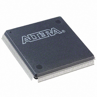
EP3C16Q240C8N Altera, EP3C16Q240C8N Datasheet - Page 83

EP3C16Q240C8N
Manufacturer Part Number
EP3C16Q240C8N
Description
IC CYCLONE III FPGA 16K 240PQFP
Manufacturer
Altera
Series
Cyclone® IIIr
Datasheets
1.EP3C5F256C8N.pdf
(5 pages)
2.EP3C5F256C8N.pdf
(34 pages)
3.EP3C5F256C8N.pdf
(66 pages)
4.EP3C5F256C8N.pdf
(14 pages)
5.EP3C5F256C8N.pdf
(76 pages)
6.EP3C16Q240C8N.pdf
(274 pages)
Specifications of EP3C16Q240C8N
Number Of Logic Elements/cells
15408
Number Of Labs/clbs
963
Total Ram Bits
516096
Number Of I /o
160
Voltage - Supply
1.15 V ~ 1.25 V
Mounting Type
Surface Mount
Operating Temperature
0°C ~ 85°C
Package / Case
240-MQFP, 240-PQFP
Family Name
Cyclone III
Number Of Logic Blocks/elements
15408
# I/os (max)
92
Frequency (max)
402MHz
Process Technology
65nm
Operating Supply Voltage (typ)
1.2V
Logic Cells
15408
Ram Bits
516096
Operating Supply Voltage (min)
1.15V
Operating Supply Voltage (max)
1.25V
Operating Temp Range
0C to 85C
Operating Temperature Classification
Commercial
Mounting
Surface Mount
Pin Count
240
Package Type
PQFP
For Use With
544-2601 - KIT DEV CYCLONE III LS EP3CLS200P0037 - BOARD DEV/EDUCATION ALTERA DE0544-2411 - KIT DEV NIOS II CYCLONE III ED.
Lead Free Status / RoHS Status
Lead free / RoHS Compliant
Number Of Gates
-
Lead Free Status / Rohs Status
Compliant
Other names
544-2458
Available stocks
Company
Part Number
Manufacturer
Quantity
Price
Company:
Part Number:
EP3C16Q240C8N
Manufacturer:
ALTERA64
Quantity:
74
Chapter 5: Clock Networks and PLLs in the Cyclone III Device Family
Hardware Features
© December 2009
Altera Corporation
There are two ways to use the clock switchover feature:
■
■
Figure 5–15
automatic loss of clock detection. Here, the inclk0 signal remains low. After the
inclk0 signal remains low for approximately two clock cycles, the clock-sense
circuitry drives the clkbad[0] signal high. Also, because the reference clock signal is
not toggling, the switchover state machine controls the multiplexer through the
clksw signal to switch to inclk1.
Figure 5–15. Automatic Switchover Upon Clock Loss Detection
Note to
(1) Switchover is enabled on the falling edge of inclk0 or inclk1, depending on which clock is available. In this
Use the switchover circuitry for switching from inclk0 to inclk1 running at the
same frequency. For example, in applications that require a redundant clock with
the same frequency as the reference clock, the switchover state machine generates
a signal that controls the multiplexer select input shown in
case, inclk1 becomes the reference clock for the PLL. This automatic switchover
can switch back and forth between the inclk0 and inclk1 clocks any number of
times, when one of the two clocks fails and the other clock is available.
Use the clkswitch input for user- or system-controlled switch conditions. This is
possible for same-frequency switchover or to switch between inputs of different
frequencies. For example, if inclk0 is 66 MHz and inclk1 is 200 MHz, you must
control the switchover because the automatic clock-sense circuitry cannot monitor
primary and secondary clock frequencies with a frequency difference of more than
20%. This feature is useful when clock sources can originate from multiple cards
on the backplane, requiring a system-controlled switchover between frequencies
of operation. Choose the secondary clock frequency so the VCO operates in the
recommended frequency range. Also, set the M, N, and C counters accordingly to
keep the VCO operating frequency in the recommended range.
figure, switchover is enabled on the falling edge of inclk1.
Figure
5–15:
shows a waveform example of the switchover feature when using
activeclock
clkbad0
clkbad1
muxout
inclk0
inclk1
(1)
(Note 1)
Cyclone III Device Handbook, Volume 1
Figure
5–14. In this
5–19


