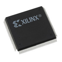
XC4005L-5PQ208C Xilinx Inc, XC4005L-5PQ208C Datasheet - Page 81

XC4005L-5PQ208C
Manufacturer Part Number
XC4005L-5PQ208C
Description
IC 3.3V FPGA 196 CLB'S 208-PQFP
Manufacturer
Xilinx Inc
Series
XC4000r
Datasheet
1.XC4005L-5PC84C.pdf
(175 pages)
Specifications of XC4005L-5PQ208C
Number Of Logic Elements/cells
466
Number Of Labs/clbs
196
Total Ram Bits
6272
Number Of I /o
112
Number Of Gates
5000
Voltage - Supply
3 V ~ 3.6 V
Mounting Type
Surface Mount
Operating Temperature
0°C ~ 85°C
Package / Case
208-BFQFP
Lead Free Status / RoHS Status
Contains lead / RoHS non-compliant
Other names
122-1122
Available stocks
Company
Part Number
Manufacturer
Quantity
Price
- Current page: 81 of 175
- Download datasheet (2Mb)
XC4000E CLB Switching Characteristic Guidelines
Testing of the switching parameters is modeled after testing methods specified by MIL-M-38510/605. All devices are 100%
functionally tested. Internal timing parameters are not measured directly. They are derived from benchmark timing patterns
that are taken at device introduction, prior to any process improvements. For more detailed, more precise, and more up-to-
date information, use the values provided by the XACT timing calculator and used in the simulator. These values can be
printed in tabular format by running LCA2XNF -S.
The following guidelines reflect worst-case values over the recommended operating conditions. They are expressed in units
of nanoseconds and apply to all XC4000E devices unless otherwise noted.
September 18, 1996 (Version 1.04)
Combinatorial Delays
F/G inputs to X/Y outputs
F/G inputs via H’ to X/Y outputs
C inputs via SR through H’ to X/Y outputs
C inputs via H’ to X/Y outputs
C inputs via DIN through H’ to X/Y outputs
CLB Fast Carry Logic
Operand inputs (F1, F2, G1, G4) to COUT
Add/Subtract input (F3) to COUT
Initialization inputs (F1, F3) to COUT
CIN through function generators to
CIN to COUT, bypass function generators
Sequential Delays
Clock K to outputs Q
Setup Time before Clock K
F/G inputs
F/G inputs via H’
C inputs via H0 through H’
C inputs via H1 through H’
C inputs via H2 through H’
C inputs via DIN
C inputs via EC
C inputs via S/R, going Low (inactive)
C
C
IN
IN
X/Y outputs
input via F’/G’
input via F’/G’ and H’
Description
Speed Grade
Symbol
T
T
T
T
T
T
T
T
T
T
T
T
T
T
T
T
T
T
T
HH0CK
HH1CK
HH2CK
T
T
HH0O
HH1O
HH2O
OPCY
ECCK
CHCK
ASCY
INCY
IHCK
DICK
SUM
CKO
RCK
CCK
BYP
IHO
ILO
ICK
Min
4.0
6.1
4.5
5.0
4.8
3.0
4.0
4.2
-4
Max
2.7
4.7
4.1
3.7
4.5
3.2
5.5
1.7
3.8
1.0
3.7
Min
3.0
4.6
3.6
4.1
3.8
2.4
3.0
4.0
-3
Max
2.0
4.3
3.3
3.6
3.6
2.6
4.4
1.7
3.3
0.7
2.8
Min
Preliminary
2.4
3.9
3.5
3.3
3.7
2.0
2.6
4.0
-2
Max
1.6
2.7
2.4
2.2
2.6
2.1
3.7
1.4
2.6
0.6
2.8
4-85
Related parts for XC4005L-5PQ208C
Image
Part Number
Description
Manufacturer
Datasheet
Request
R

Part Number:
Description:
IC 3.3V FPGA 196 CLB'S 100-PQFP
Manufacturer:
Xilinx Inc
Datasheet:

Part Number:
Description:
IC 3.3V FPGA 196 CLB'S 84-PLCC
Manufacturer:
Xilinx Inc
Datasheet:

Part Number:
Description:
IC LOGIC CL ARRAY 5000GAT 160PQF
Manufacturer:
Xilinx Inc
Datasheet:

Part Number:
Description:
IC LOGIC CL ARRAY 5000GAT 208PQ
Manufacturer:
Xilinx Inc
Datasheet:

Part Number:
Description:
IC LOGIC CL ARRAY 5000GAT 84PLC
Manufacturer:
Xilinx Inc
Datasheet:

Part Number:
Description:
FPGA XC4000 Family 5K Gates 196 Cells 100MHz CMOS Technology 5V 160-Pin PQFP
Manufacturer:
Xilinx Inc

Part Number:
Description:
FPGA XC4000 Family 5K Gates 196 Cells 100MHz CMOS Technology 5V 84-Pin PLCC
Manufacturer:
Xilinx Inc

Part Number:
Description:
IC CPLD .8K 36MCELL 44-VQFP
Manufacturer:
Xilinx Inc
Datasheet:

Part Number:
Description:
IC CPLD 72MCRCELL 10NS 44VQFP
Manufacturer:
Xilinx Inc
Datasheet:

Part Number:
Description:
IC CPLD 1.6K 72MCELL 64-VQFP
Manufacturer:
Xilinx Inc
Datasheet:

Part Number:
Description:
IC CR-II CPLD 64MCELL 44-VQFP
Manufacturer:
Xilinx Inc
Datasheet:

Part Number:
Description:
IC CPLD 1.6K 72MCELL 100-TQFP
Manufacturer:
Xilinx Inc
Datasheet:

Part Number:
Description:
IC CR-II CPLD 64MCELL 56-BGA
Manufacturer:
Xilinx Inc
Datasheet:

Part Number:
Description:
IC CPLD 72MCRCELL 7.5NS 44VQFP
Manufacturer:
Xilinx Inc
Datasheet:

Part Number:
Description:
IC CR-II CPLD 64MCELL 100-VQFP
Manufacturer:
Xilinx Inc
Datasheet:


