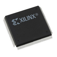
XC4005L-5PQ208C Xilinx Inc, XC4005L-5PQ208C Datasheet - Page 76

XC4005L-5PQ208C
Manufacturer Part Number
XC4005L-5PQ208C
Description
IC 3.3V FPGA 196 CLB'S 208-PQFP
Manufacturer
Xilinx Inc
Series
XC4000r
Datasheet
1.XC4005L-5PC84C.pdf
(175 pages)
Specifications of XC4005L-5PQ208C
Number Of Logic Elements/cells
466
Number Of Labs/clbs
196
Total Ram Bits
6272
Number Of I /o
112
Number Of Gates
5000
Voltage - Supply
3 V ~ 3.6 V
Mounting Type
Surface Mount
Operating Temperature
0°C ~ 85°C
Package / Case
208-BFQFP
Lead Free Status / RoHS Status
Contains lead / RoHS non-compliant
Other names
122-1122
Available stocks
Company
Part Number
Manufacturer
Quantity
Price
- Current page: 76 of 175
- Download datasheet (2Mb)
XC4000 Series Field Programmable Gate Arrays
XC4000E Switching Characteristics
Definition of Terms
In the following tables, some specifications may be designated as Advance or Preliminary. These terms are defined as
follows:
Advance:
Preliminary: Based on preliminary characterization. Further changes are not expected.
Unmarked:
XC4000E Operating Conditions
Note 1:
Note 2:
Note 3:
XC4000E DC Characteristics Over Operating Conditions
Note 1:
Note 2:
1. Notwithstanding the definition of the above terms, all specifications are subject to change without notice.
4-80
V
V
V
T
V
V
I
I
C
I
I
CCO
L
RIN
RLL
IN
CC
IH
IL
OH
OL
IN
Symbol
Symbol
At junction temperatures above those listed as Operating Conditions, all delay parameters increase by 0.35% per C.
Typical value only. Not tested or characterized.
Input and output measurement thresholds for TTL are 1.5 V. Input and output measurement thresholds for CMOS are 2.5 V.
With 50% of the outputs simultaneously sinking 12mA, up to a maximum of 64 pins.
With no output current loads, no active input or Longline pull-up resistors, all package pins at Vcc or GND, and the FPGA
configured with a MakeBits Tie option.
Supply voltage relative to GND, T
Supply voltage relative to GND, T
Supply voltage relative to GND, T
High-level input voltage
Low-level input voltage
Input signal transition time (Note 2)
High-level output voltage @ I
High-level output voltage @ I
Low-level output voltage @ I
(Note 1)
Quiescent FPGA supply current (Note 2)
Input or output leakage current
Input capacitance (sample tested)
Pad pull-up (when selected) @ V
Horizontal Longline pull-up (when selected) @ logic Low
Specifications not identified as either Advance or Preliminary are to be considered Final.
Initial estimates based on simulation and/or extrapolation from other speed grades, devices, or device
families. Use as estimates, not for production.
OL
OH
OH
= 12.0mA, V
Description
Description
= -4.0mA, V
= -1.0mA, V
IN
J
J
C
= 0V (sample tested)
= -0 C to +85 C
= -40 C to +100 C
= -55 C to +125 C Military
CC
CC
CC
min
min
min
Commercial
Industrial
TTL inputs
CMOS inputs
TTL inputs
CMOS inputs
TTL outputs
CMOS outputs
TTL outputs
CMOS outputs
TTL input levels
CMOS input levels
PQFP and MQFP
packages
Other packages
September 18, 1996 (Version 1.04)
V
CC
4.75
70%
0.02
Min
Min
-10
4.5
4.5
2.0
2.4
0.2
0
0
-0.5
1
100%
20%
Max
0.25
Max
5.25
V
+10
250
5.5
5.5
0.8
0.4
0.4
2.5
10
10
16
1
CC
Units
Units
V
V
mA
mA
mA
mA
pF
pF
ns
V
V
V
V
V
V
V
V
V
CC
CC
A
Related parts for XC4005L-5PQ208C
Image
Part Number
Description
Manufacturer
Datasheet
Request
R

Part Number:
Description:
IC 3.3V FPGA 196 CLB'S 100-PQFP
Manufacturer:
Xilinx Inc
Datasheet:

Part Number:
Description:
IC 3.3V FPGA 196 CLB'S 84-PLCC
Manufacturer:
Xilinx Inc
Datasheet:

Part Number:
Description:
IC LOGIC CL ARRAY 5000GAT 160PQF
Manufacturer:
Xilinx Inc
Datasheet:

Part Number:
Description:
IC LOGIC CL ARRAY 5000GAT 208PQ
Manufacturer:
Xilinx Inc
Datasheet:

Part Number:
Description:
IC LOGIC CL ARRAY 5000GAT 84PLC
Manufacturer:
Xilinx Inc
Datasheet:

Part Number:
Description:
FPGA XC4000 Family 5K Gates 196 Cells 100MHz CMOS Technology 5V 160-Pin PQFP
Manufacturer:
Xilinx Inc

Part Number:
Description:
FPGA XC4000 Family 5K Gates 196 Cells 100MHz CMOS Technology 5V 84-Pin PLCC
Manufacturer:
Xilinx Inc

Part Number:
Description:
IC CPLD .8K 36MCELL 44-VQFP
Manufacturer:
Xilinx Inc
Datasheet:

Part Number:
Description:
IC CPLD 72MCRCELL 10NS 44VQFP
Manufacturer:
Xilinx Inc
Datasheet:

Part Number:
Description:
IC CPLD 1.6K 72MCELL 64-VQFP
Manufacturer:
Xilinx Inc
Datasheet:

Part Number:
Description:
IC CR-II CPLD 64MCELL 44-VQFP
Manufacturer:
Xilinx Inc
Datasheet:

Part Number:
Description:
IC CPLD 1.6K 72MCELL 100-TQFP
Manufacturer:
Xilinx Inc
Datasheet:

Part Number:
Description:
IC CR-II CPLD 64MCELL 56-BGA
Manufacturer:
Xilinx Inc
Datasheet:

Part Number:
Description:
IC CPLD 72MCRCELL 7.5NS 44VQFP
Manufacturer:
Xilinx Inc
Datasheet:

Part Number:
Description:
IC CR-II CPLD 64MCELL 100-VQFP
Manufacturer:
Xilinx Inc
Datasheet:


