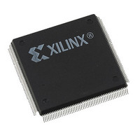
XC4005L-5PQ208C Xilinx Inc, XC4005L-5PQ208C Datasheet - Page 37

XC4005L-5PQ208C
Manufacturer Part Number
XC4005L-5PQ208C
Description
IC 3.3V FPGA 196 CLB'S 208-PQFP
Manufacturer
Xilinx Inc
Series
XC4000r
Datasheet
1.XC4005L-5PC84C.pdf
(175 pages)
Specifications of XC4005L-5PQ208C
Number Of Logic Elements/cells
466
Number Of Labs/clbs
196
Total Ram Bits
6272
Number Of I /o
112
Number Of Gates
5000
Voltage - Supply
3 V ~ 3.6 V
Mounting Type
Surface Mount
Operating Temperature
0°C ~ 85°C
Package / Case
208-BFQFP
Lead Free Status / RoHS Status
Contains lead / RoHS non-compliant
Other names
122-1122
Available stocks
Company
Part Number
Manufacturer
Quantity
Price
Global Nets and Buffers
Both the XC4000E and the XC4000EX have dedicated glo-
bal networks. These networks are designed to distribute
clocks and other high fanout control signals throughout the
devices with minimal skew.
described in detail in the following sections.
descriptions and diagrams are summarized in
The table shows which CLB and IOB clock pins can be
sourced by which global buffers.
In both XC4000E and XC4000EX devices, placement of a
library symbol called BUFG results in the software choos-
ing the appropriate clock buffer, based on the timing
requirements of the design. The detailed information in
these sections is included only for reference.
Global Nets and Buffers (XC4000E only)
Four vertical longlines in each CLB column are driven
exclusively by special global buffers.
in addition to the vertical longlines used for standard inter-
connect. The four global lines can be driven by either of
two types of global buffers. The clock pins of every CLB
and IOB can also be sourced from local interconnect.
Two different types of clock buffers are available in the
XC4000E:
• Primary Global Buffers (BUFGP)
• Secondary Global Buffers (BUFGS)
Table 17: Clock Pin Access
L = Left, R = Right, T = Top, B = Bottom
September 18, 1996 (Version 1.04)
All CLBs in Quadrant
All CLBs in Device
IOBs on Adjacent Vertical
Half Edge
IOBs on Adjacent Vertical
Full Edge
IOBs on Adjacent Horizontal
Half Edge (Direct)
IOBs on Adjacent Horizontal
Half Edge (through CLB globals)
IOBs on Adjacent Horizontal
Full Edge (through CLB globals)
The global buffers are
These longlines are
BUFGP
XC4000E
Table
The text
BUFGS
17.
Four Primary Global buffers offer the shortest delay and
negligible skew.
slightly longer delay and slightly more skew due to poten-
tially heavier loading, but offer greater flexibility when used
to drive non-clock CLB inputs.
The Primary Global buffers must be driven by the semi-
dedicated pads. The Secondary Global buffers can be
sourced by either semi-dedicated pads or internal nets.
Each CLB column has four dedicated vertical Global lines.
Each of these lines can be accessed by one particular Pri-
mary Global buffer, or by any of the Secondary Global buff-
ers, as shown in
one Primary buffer and one Secondary buffer.
IOBs along the left and right edges have four vertical global
longlines. Top and bottom IOBs can be clocked from the
global lines in the adjacent CLB column.
A global buffer should be specified for all timing-sensitive
global signal distribution. To use a global buffer, place a
BUFGP (primary buffer), BUFGS (secondary buffer), or
BUFG (either primary or secondary buffer) element in a
schematic or in HDL code.
attribute or property to direct placement to the designated
location. For example, attach a LOC=L attribute or property
to a BUFGS symbol to direct that a buffer be placed in one
of the two Secondary Global buffers on the left edge of the
device, or a LOC=BL to indicate the Secondary Global
buffer on the bottom edge of the device, on the left.
BUFGLS
BUFGE
L & R
Figure
XC4000EX
Four Secondary Global buffers have
35. Each corner of the device has
BUFGE
T & B
If desired, attach a LOC
BUFFCL
K
connect
Local
Inter-
4-41


