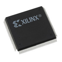
XC4005L-5PQ208C Xilinx Inc, XC4005L-5PQ208C Datasheet - Page 26

XC4005L-5PQ208C
Manufacturer Part Number
XC4005L-5PQ208C
Description
IC 3.3V FPGA 196 CLB'S 208-PQFP
Manufacturer
Xilinx Inc
Series
XC4000r
Datasheet
1.XC4005L-5PC84C.pdf
(175 pages)
Specifications of XC4005L-5PQ208C
Number Of Logic Elements/cells
466
Number Of Labs/clbs
196
Total Ram Bits
6272
Number Of I /o
112
Number Of Gates
5000
Voltage - Supply
3 V ~ 3.6 V
Mounting Type
Surface Mount
Operating Temperature
0°C ~ 85°C
Package / Case
208-BFQFP
Lead Free Status / RoHS Status
Contains lead / RoHS non-compliant
Other names
122-1122
Available stocks
Company
Part Number
Manufacturer
Quantity
Price
XC4000 Series Field Programmable Gate Arrays
The buffer enable is an active-High 3-state (i.e. an active-
Low enable), as shown in
Another 3-state buffer with similar access is located near
each I/O block along the right and left edges of the array.
(See
The horizontal longlines driven by the 3-state buffers have a
weak keeper at each end. This circuit prevents undefined
floating levels. However, it is overridden by any driver, even
a pull-up resistor.
Special longlines running along the perimeter of the array
can be used to wire-AND signals coming from nearby IOBs
or from internal longlines. These longlines form the wide
edge decoders discussed in
page
Three-State Buffer Modes
The 3-state buffers can be configured in three modes:
• Standard 3-state buffer
• Wired-AND with input on the I pin
• Wired OR-AND
Standard 3-State Buffer
All three pins are used. Place the library element BUFT.
Connect the input to the I pin and the output to the O pin.
The T pin is an active-High 3-state (i.e. an active-Low
enable). Tie the T pin to Ground to implement a standard
buffer.
Wired-AND with Input on the I Pin
The buffer can be used as a Wired-AND. Use the WAND1
library symbol, which is essentially an open-drain buffer.
4-30
Figure 22: Open-Drain Buffers Implement a Wired-AND Function
Figure 23: 3-State Buffers Implement a Multiplexer
Figure 33 on page
31.
"Weak Keeper"
D
A
WAND1
~100 k
39.)
Table
“Wide Edge Decoders” on
15.
D
B
D
A
A
WAND1
BUFT
Z = D
D
D
D
C
D
Z = D
A
B
B
D
W0R2AND
B
A
WAND4, WAND8, and WAND16 are also available. See
the XACT Libraries Guide for further information.
The T pin is internally tied to the I pin. Connect the input to
the I pin and the output to the O pin. Connect the outputs of
all the WAND1s together and attach a PULLUP symbol.
Wired OR-AND
The buffer can be configured as a Wired OR-AND. A High
level on either input turns off the output.
WOR2AND library symbol, which is essentially an open-
drain 2-input OR gate. The two input pins are functionally
equivalent. Attach the two inputs to the I0 and I1 pins and
tie the output to the O pin. Tie the outputs of all the
WOR2ANDs together and attach a PULLUP symbol.
Three-State Buffer Examples
Figure 22
ment a wired-AND function. When all the buffer inputs are
High, the pull-up resistor(s) provide the High output.
Figure 23
ment a multiplexer. The selection is accomplished by the
buffer 3-state signal.
Pay particular attention to the polarity of the T pin when
using these buffers in a design. Active-High 3-state (T) is
identical to an active-Low output enable, as shown in
Table
Table 15: Three-State Buffer Functionality
• A + D
(D
C
+D
BUFT
D
B
) (D
15.
• B + D
E
IN
IN
X
+D
shows how to use the 3-state buffers to imple-
shows how to use the 3-state buffers to imple-
C
F
)
• C + D
D
C
C
N
D
D
• N
E
F
W0R2AND
BUFT
September 18, 1996 (Version 1.04)
T
1
0
D
N
N
P
U
L
L
BUFT
X6465
U
P
X6466
OUT
IN
Z
Use the


