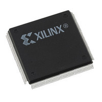
XC4005L-5PQ208C Xilinx Inc, XC4005L-5PQ208C Datasheet - Page 40

XC4005L-5PQ208C
Manufacturer Part Number
XC4005L-5PQ208C
Description
IC 3.3V FPGA 196 CLB'S 208-PQFP
Manufacturer
Xilinx Inc
Series
XC4000r
Datasheet
1.XC4005L-5PC84C.pdf
(175 pages)
Specifications of XC4005L-5PQ208C
Number Of Logic Elements/cells
466
Number Of Labs/clbs
196
Total Ram Bits
6272
Number Of I /o
112
Number Of Gates
5000
Voltage - Supply
3 V ~ 3.6 V
Mounting Type
Surface Mount
Operating Temperature
0°C ~ 85°C
Package / Case
208-BFQFP
Lead Free Status / RoHS Status
Contains lead / RoHS non-compliant
Other names
122-1122
Available stocks
Company
Part Number
Manufacturer
Quantity
Price
XC4000 Series Field Programmable Gate Arrays
Global Early Buffers
Each corner of the XC4000EX device has two Global Early
buffers. The primary purpose of the Global Early buffers is
to provide an earlier clock access than the potentially
heavily-loaded Global Low-Skew buffers. A clock source
applied to both buffers will result in the Global Early clock
edge occurring several nanoseconds earlier than the Glo-
bal Low-Skew buffer clock edge, due to the lighter loading.
Global Early buffers also facilitate the fast capture of device
inputs, using the Fast Capture latches described in
Input Signals” on page
clock signal, and route it through both a Global Early buffer
and a Global Low-Skew buffer. (The two buffers share an
input pad.) Use the Global Early buffer to clock the Fast
Capture latch, and the Global Low-Skew buffer to clock the
normal input flip-flop or latch, as shown in
page
The Global Early buffers can also be used to provide a fast
Clock-to-Out on device output pins. However, an early
clock in the output flip-flop IOB must be taken into consid-
eration when calculating the internal clock speed for the
design.
The Global Early buffers at the left and right edges of the
chip have slightly different capabilities than the ones at the
top and bottom.
Figure 36 on page 42
tion.
Each Global Early buffer can access the eight vertical Glo-
bal lines for all CLBs in the quadrant. Therefore, only one-
fourth of the CLB clock pins can be accessed. This restric-
tion is in large part responsible for the faster speed of the
buffers, relative to the Global Low-Skew buffers.
4-44
Figure 37: Any BUFGLS (GCK1 - GCK8) Can
Drive Any or All Clock Inputs on the Device
1
2
O
O
B
B
26.
I
I
8
3
CLB
CLB
IOB
IOB
Refer to
while reading the following explana-
24. For Fast Capture, take a single
Figure
CLB
CLB
IOB
IOB
38,
Figure
Figure 18 on
7
4
X6753
O
O
B
B
I
I
39, and
6
5
“IOB
The left-side Global Early buffers can each drive two of the
four vertical lines accessing the IOBs on the entire left edge
of the device. The right-side Global Early buffers can each
drive two of the eight vertical lines accessing the IOBs on
the entire right edge of the device. (See
Each left and right Global Early buffer can also drive half of
the IOBs along either the top or bottom edge of the device,
using a dedicated line that can only be accessed through
the Global Early buffers.
The top and bottom Global Early buffers can drive half of
the IOBs along either the left or right edge of the device, as
shown in
tom IOBs via the CLB global lines.
Figure 39: Top and Bottom BUFGEs Can Drive Any
or All Clock Inputs in Same Quadrant (GCK8 is
shown. GCK3, GCK4 and GCK7 are similar.)
Figure 38: Left and Right BUFGEs Can Drive Any or
All Clock Inputs in Same Quadrant or Edge (GCK1 is
shown. GCK2, GCK5 and GCK6 are similar.)
1
2
1
2
O
O
B
B
I
I
O
O
B
B
I
I
8
3
Figure
8
3
39. They can only access the top and bot-
CLB
CLB
CLB
CLB
IOB
IOB
IOB
IOB
September 18, 1996 (Version 1.04)
CLB
CLB
IOB
IOB
CLB
CLB
IOB
IOB
Figure
38.)
7
4
7
4
X6747
O
O
X6751
B
B
I
I
O
O
B
B
I
I
6
5
6
5


