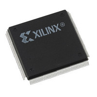
XC4005L-5PQ208C Xilinx Inc, XC4005L-5PQ208C Datasheet - Page 62

XC4005L-5PQ208C
Manufacturer Part Number
XC4005L-5PQ208C
Description
IC 3.3V FPGA 196 CLB'S 208-PQFP
Manufacturer
Xilinx Inc
Series
XC4000r
Datasheet
1.XC4005L-5PC84C.pdf
(175 pages)
Specifications of XC4005L-5PQ208C
Number Of Logic Elements/cells
466
Number Of Labs/clbs
196
Total Ram Bits
6272
Number Of I /o
112
Number Of Gates
5000
Voltage - Supply
3 V ~ 3.6 V
Mounting Type
Surface Mount
Operating Temperature
0°C ~ 85°C
Package / Case
208-BFQFP
Lead Free Status / RoHS Status
Contains lead / RoHS non-compliant
Other names
122-1122
Available stocks
Company
Part Number
Manufacturer
Quantity
Price
- Current page: 62 of 175
- Download datasheet (2Mb)
XC4000 Series Field Programmable Gate Arrays
Configuration Timing
The seven configuration modes are discussed in detail in
this section. Timing specifications are included.
Master Serial Mode
In Master Serial mode, the CCLK output of the lead FPGA
drives a Xilinx Serial PROM that feeds the FPGA DIN input.
Each rising edge of the CCLK output increments the Serial
PROM internal address counter. The next data bit is put on
the SPROM data output, connected to the FPGA DIN pin.
The lead FPGA accepts this data on the subsequent rising
CCLK edge.
The lead FPGA then presents the preamble data—and all
data that overflows the lead device—on its DOUT pin.
There is an internal pipeline delay of 1.5 CCLK periods,
which means that DOUT changes on the falling CCLK
edge, and the next FPGA in the daisy chain accepts data
on the subsequent rising CCLK edge.
4-66
Figure 53: Master Serial Mode Circuit Diagram
PROGRAM
NOTE:
M2, M1, M0 can be shorted
to Ground if not used as I/O
4.7 K
4.7 K
M2
PROGRAM
DONE
M0 M1
XC4000E/EX
MASTER
SERIAL
4.7 K
DOUT
CCLK
LDC
INIT
DIN
V
CC
4.7 K
(Low Reset Option Used)
CLK
DATA
CE
RESET/OE
XC1700D
CEO
VPP
+5 V
In MakeBits, the user can specify Fast ConfigRate, which,
starting several bits into the first frame, increases the CCLK
frequency by a factor of eight. The value increases from
between 0.5 and 1.25 MHz, to a value between 4 and 10
MHz. (For low-voltage devices, the frequency can be up to
10% lower.) Be sure that the serial PROM and slaves are
fast enough to support this data rate. XC2000, XC3000/A,
and XC3100A devices do not support the Fast ConfigRate
option.
The SPROM CE input can be driven from either LDC or
DONE. Using LDC avoids potential contention on the DIN
pin, if this pin is configured as user-I/O, but LDC is then
restricted to be a permanently High user output after con-
figuration. Using DONE can also avoid contention on DIN,
provided the early DONE option is invoked.
Figure 53
device is in Master Serial mode.
Master Serial mode is selected by a <000> on the mode
pins (M2, M1, M0).
N/C
PROGRAM
DONE
M2
DIN
CCLK
M0 M1
XC4000E/EX,
N/C
XC5200
SLAVE
shows a full master/slave system. The leftmost
DOUT
INIT
September 18, 1996 (Version 1.04)
V
4.7 K
CC
4.7 K
NOTE:
M2, M1, M0 can be shorted
to V
M2
DIN
CCLK
RESET
D/P
CC
M0
if not used as I/O
XC3100A
M1
SLAVE
4.7 K
PWRDN
DOUT
INIT
X6608
Related parts for XC4005L-5PQ208C
Image
Part Number
Description
Manufacturer
Datasheet
Request
R

Part Number:
Description:
IC 3.3V FPGA 196 CLB'S 100-PQFP
Manufacturer:
Xilinx Inc
Datasheet:

Part Number:
Description:
IC 3.3V FPGA 196 CLB'S 84-PLCC
Manufacturer:
Xilinx Inc
Datasheet:

Part Number:
Description:
IC LOGIC CL ARRAY 5000GAT 160PQF
Manufacturer:
Xilinx Inc
Datasheet:

Part Number:
Description:
IC LOGIC CL ARRAY 5000GAT 208PQ
Manufacturer:
Xilinx Inc
Datasheet:

Part Number:
Description:
IC LOGIC CL ARRAY 5000GAT 84PLC
Manufacturer:
Xilinx Inc
Datasheet:

Part Number:
Description:
FPGA XC4000 Family 5K Gates 196 Cells 100MHz CMOS Technology 5V 160-Pin PQFP
Manufacturer:
Xilinx Inc

Part Number:
Description:
FPGA XC4000 Family 5K Gates 196 Cells 100MHz CMOS Technology 5V 84-Pin PLCC
Manufacturer:
Xilinx Inc

Part Number:
Description:
IC CPLD .8K 36MCELL 44-VQFP
Manufacturer:
Xilinx Inc
Datasheet:

Part Number:
Description:
IC CPLD 72MCRCELL 10NS 44VQFP
Manufacturer:
Xilinx Inc
Datasheet:

Part Number:
Description:
IC CPLD 1.6K 72MCELL 64-VQFP
Manufacturer:
Xilinx Inc
Datasheet:

Part Number:
Description:
IC CR-II CPLD 64MCELL 44-VQFP
Manufacturer:
Xilinx Inc
Datasheet:

Part Number:
Description:
IC CPLD 1.6K 72MCELL 100-TQFP
Manufacturer:
Xilinx Inc
Datasheet:

Part Number:
Description:
IC CR-II CPLD 64MCELL 56-BGA
Manufacturer:
Xilinx Inc
Datasheet:

Part Number:
Description:
IC CPLD 72MCRCELL 7.5NS 44VQFP
Manufacturer:
Xilinx Inc
Datasheet:

Part Number:
Description:
IC CR-II CPLD 64MCELL 100-VQFP
Manufacturer:
Xilinx Inc
Datasheet:


