ADAU1445YSVZ-3A-RL Analog Devices Inc, ADAU1445YSVZ-3A-RL Datasheet - Page 85
ADAU1445YSVZ-3A-RL
Manufacturer Part Number
ADAU1445YSVZ-3A-RL
Description
175MHZ SigmaDSP,2x8 SRCs
Manufacturer
Analog Devices Inc
Series
SigmaDSP®r
Type
Audio Processorr
Specifications of ADAU1445YSVZ-3A-RL
Applications
Automotive Audio
Mounting Type
Surface Mount
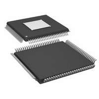
Package / Case
100-TQFP Exposed Pad, 100-eTQFP, 100-HTQFP, 100-VQFP
Format
Fixed Point
Program Memory Size
Not RequiredKB
Operating Supply Voltage (typ)
1.8/3.3V
Operating Temp Range
-40C to 105C
Operating Temperature Classification
Industrial
Mounting
Surface Mount
Pin Count
100
Lead Free Status / RoHS Status
Lead free / RoHS Compliant
Lead Free Status / RoHS Status
Lead free / RoHS Compliant
Available stocks
Company
Part Number
Manufacturer
Quantity
Price
Company:

Part Number:
ADAU1445YSVZ-3A-RL
Manufacturer:
Analog Devices Inc
Quantity:
10 000


APPLICATIONS INFORMATION
LAYOUT RECOMMENDATIONS
Parts Placement
All 100 nF bypass capacitors, which are recommended for every
analog, digital, and PLL power-ground pair, should be placed as
close to the ADAU1445/ADAU1446 as possible. The AVDD,
DVDD, PVDD, and IOVDD supply signals on the board should
each be bypassed with an additional single bulk capacitor (10 μF
to 47 μF).
All traces in the crystal oscillator circuit (Figure 9) should be
kept as short as possible to minimize stray capacitance. There
should not be any long board traces connected to crystal
oscillator circuit components because such traces may affect
crystal startup and operation.
Grounding
A single ground plane should be used in the application layout.
Components in an analog signal path should be placed away
from digital signals.
Exposed Pad PCB Design
The ADAU1445 package includes an exposed pad for improved
heat dissipation. When designing a board for such a package,
special consideration should be given to the following:
•
•
A copper layer equal in size to the exposed pad should be
on all layers of the board, from top to bottom, and should
connect somewhere to a dedicated copper board layer (see
Figure 60).
Vias should be placed to connect all layers of copper, allowing
for efficient heat and energy conductivity. For an example,
see Figure 61, which has 16 vias arranged in a 4 × 4 grid in
the pad area.
Figure 60. Exposed Pad Layout Example—Side View
VIAS
COPPER SQUARES
TOP
GROUND
POWER
BOTTOM
Rev. A | Page 85 of 92
PLL Loop Filter
The single resistor and two capacitors in the PLL loop filter
should be connected to the PLL_FILT and PVDD pins with
short traces to minimize jitter.
Power Supply Bypass Capacitors
Each power supply pin should be bypassed to its nearest
appropriate ground pin with a single 100 nF capacitor. The
connections to each side of the capacitor should be as short as
possible, and the trace should stay on a single layer with no vias.
For maximum effectiveness, the capacitor should preferably be
located either equidistant from the power and ground pins or,
when equidistant placement is not possible, slightly closer to the
power pin. Thermal connections to the planes should be made
on the far side of the capacitor.
EOS/ESD Protection
Although the ADAU1445/ADAU1446 have robust internal
protection circuitry against overvoltages and electrostatic
discharge, an external transient voltage suppressor (TVS) is
recommended for all systems to prevent damage to the IC.
Examples can be found in the AN-311 Application Note on the
Analog Devices website.
Figure 62. Recommended Power Supply Bypass Capacitor Layout
Figure 61. Exposed Pad Layout Example—Top View
TO POWER
CAPACITOR
POWER GROUND
ADAU1445/ADAU1446
TO GROUND
Related parts for ADAU1445YSVZ-3A-RL
Image
Part Number
Description
Manufacturer
Datasheet
Request
R

Part Number:
Description:
SigmaDSP� Digital Audio Processor with Flexible Audio Routing Matrix
Manufacturer:
Analog Devices
Datasheet:

Part Number:
Description:
±1.7g Dual-Axis IMEMS Accelerometer Evaluation Board
Manufacturer:
Analog Devices Inc
Datasheet:

Part Number:
Description:
Inertial Sensor Evaluation System
Manufacturer:
Analog Devices Inc
Datasheet:
Part Number:
Description:
Manufacturer:
Analog Devices Inc
Datasheet:
Part Number:
Description:
Manufacturer:
Analog Devices Inc
Datasheet:
Part Number:
Description:
Manufacturer:
Analog Devices Inc
Datasheet:
Part Number:
Description:
Manufacturer:
Analog Devices Inc
Datasheet:
Part Number:
Description:
Manufacturer:
Analog Devices Inc
Datasheet:
Part Number:
Description:
Manufacturer:
Analog Devices Inc
Datasheet:
Part Number:
Description:
Manufacturer:
Analog Devices Inc
Datasheet:
Part Number:
Description:
Manufacturer:
Analog Devices Inc
Datasheet:
Part Number:
Description:
Manufacturer:
Analog Devices Inc
Datasheet:
Part Number:
Description:
Manufacturer:
Analog Devices Inc
Datasheet: