ADAU1445YSVZ-3A-RL Analog Devices Inc, ADAU1445YSVZ-3A-RL Datasheet - Page 23
ADAU1445YSVZ-3A-RL
Manufacturer Part Number
ADAU1445YSVZ-3A-RL
Description
175MHZ SigmaDSP,2x8 SRCs
Manufacturer
Analog Devices Inc
Series
SigmaDSP®r
Type
Audio Processorr
Specifications of ADAU1445YSVZ-3A-RL
Applications
Automotive Audio
Mounting Type
Surface Mount
Package / Case
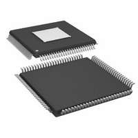
100-TQFP Exposed Pad, 100-eTQFP, 100-HTQFP, 100-VQFP
Format
Fixed Point
Program Memory Size
Not RequiredKB
Operating Supply Voltage (typ)
1.8/3.3V
Operating Temp Range
-40C to 105C
Operating Temperature Classification
Industrial
Mounting
Surface Mount
Pin Count
100
Lead Free Status / RoHS Status
Lead free / RoHS Compliant
Lead Free Status / RoHS Status
Lead free / RoHS Compliant
Available stocks
Company
Part Number
Manufacturer
Quantity
Price
Company:

Part Number:
ADAU1445YSVZ-3A-RL
Manufacturer:
Analog Devices Inc
Quantity:
10 000


VOLTAGE REGULATOR
The digital supply voltage of the ADAU1445/ADAU1446 must
be set to 1.8 V. The chip includes an on-board voltage regulator
that allows the device to be used in systems where a 1.8 V supply is
not available but a 3.3 V supply is. The only external components
needed for this are a PNP transistor and one resistor. Only one
pin, VDRIVE, is necessary to support the regulator.
The recommended design for the voltage regulator is shown
in Figure 12. The 10 μF and 100 nF capacitors shown in this
schematic are recommended for bypassing but are not necessary
for operation. Each DVDD pin should have its own 100 nF
bypass capacitor, but only one bulk capacitor (10 μF) is needed
for all pins. In this design, 3.3 V is the main system voltage; 1.8 V
is generated at the collector of the transistor, which is connected
to the DVDD pins. VDRIVE is connected to the base of the PNP
transistor. If the regulator is not used in the design, VDRIVE
can be tied to ground.
Figure 12. Voltage Regulator Design
100nF
10µF
+
DVDD
VDRIVE
ADAU1445/
ADAU1446
3.3V
1kΩ
Rev. A | Page 23 of 92
Two specifications must be considered when choosing a
regulator transistor. First, the transistor’s current amplification
factor (hFE or beta) should be at least 200. Second, the collector
of the transistor must be able to dissipate the heat generated when
regulating from 3.3 V to 1.8 V. The maximum digital current
draw of the ADAU1445, which uses ASRCs, is 310 mA. The
equation to determine the transistor’s minimum power
dissipation specifications is as follows:
Many transistors fit these specifications. Analog Devices
recommends the NJT4030P from On Semiconductor. For
projects with stringent size constraints, an FMMT734 from
Zetex can be used.
The ADAU1446, which does not contain ASRCs, has a lower
maximum digital current draw of approximately 235 mA. The
maximum power dissipation of the transistor in this case should
be around 355 mW.
SRC GROUP DELAY
The group delay of the sample rate converter is dependent on
the input and output sampling frequencies as described in the
following equations.
For f
For f
where GDS is the group delay in seconds.
(3.3 V − 1.8 V) × 310 mA = 465 mW
S_OUT
S_OUT
GDS
GDS
< f
> f
=
=
S_IN
S_IN
f
f
S
S
16
16
_
_
,
,
IN
IN
+
+
⎛
⎜
⎜
⎝
f
S
32
f
_
S
32
IN
_
IN
⎞
⎟
⎟
⎠
×
ADAU1445/ADAU1446
⎛
⎜
⎜
⎝
f
f
S
S
_
_
OUT
IN
⎞
⎟
⎟
⎠
Related parts for ADAU1445YSVZ-3A-RL
Image
Part Number
Description
Manufacturer
Datasheet
Request
R

Part Number:
Description:
SigmaDSP� Digital Audio Processor with Flexible Audio Routing Matrix
Manufacturer:
Analog Devices
Datasheet:

Part Number:
Description:
±1.7g Dual-Axis IMEMS Accelerometer Evaluation Board
Manufacturer:
Analog Devices Inc
Datasheet:

Part Number:
Description:
Inertial Sensor Evaluation System
Manufacturer:
Analog Devices Inc
Datasheet:
Part Number:
Description:
Manufacturer:
Analog Devices Inc
Datasheet:
Part Number:
Description:
Manufacturer:
Analog Devices Inc
Datasheet:
Part Number:
Description:
Manufacturer:
Analog Devices Inc
Datasheet:
Part Number:
Description:
Manufacturer:
Analog Devices Inc
Datasheet:
Part Number:
Description:
Manufacturer:
Analog Devices Inc
Datasheet:
Part Number:
Description:
Manufacturer:
Analog Devices Inc
Datasheet:
Part Number:
Description:
Manufacturer:
Analog Devices Inc
Datasheet:
Part Number:
Description:
Manufacturer:
Analog Devices Inc
Datasheet:
Part Number:
Description:
Manufacturer:
Analog Devices Inc
Datasheet:
Part Number:
Description:
Manufacturer:
Analog Devices Inc
Datasheet: