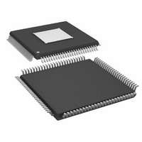
ADAU1445YSVZ-3A-RL Analog Devices Inc, ADAU1445YSVZ-3A-RL Datasheet - Page 33

ADAU1445YSVZ-3A-RL
Manufacturer Part Number
ADAU1445YSVZ-3A-RL
Description
175MHZ SigmaDSP,2x8 SRCs
Manufacturer
Analog Devices Inc
Series
SigmaDSP®r
Type
Audio Processorr
Specifications of ADAU1445YSVZ-3A-RL
Applications
Automotive Audio
Mounting Type
Surface Mount
Package / Case
100-TQFP Exposed Pad, 100-eTQFP, 100-HTQFP, 100-VQFP
Format
Fixed Point
Program Memory Size
Not RequiredKB
Operating Supply Voltage (typ)
1.8/3.3V
Operating Temp Range
-40C to 105C
Operating Temperature Classification
Industrial
Mounting
Surface Mount
Pin Count
100
Lead Free Status / RoHS Status
Lead free / RoHS Compliant
Lead Free Status / RoHS Status
Lead free / RoHS Compliant
Available stocks
Company
Part Number
Manufacturer
Quantity
Price
Company:
Part Number:
ADAU1445YSVZ-3A-RL
Manufacturer:
Analog Devices Inc
Quantity:
10 000
Serial Clock Modes and Settings
Dejitter Window Register (Address 0xE221)
Table 19. Bit Descriptions of Register 0xE221
Bit
Position
[15:6]
[5:0]
Register 0xE221 is a single 6-bit register that sets the size of the
dejitter window. The dejitter circuit prevents samples from being
repeated or omitted altogether due to jitter in the frame clock
pulses coming from the serial ports in slave mode.
The dejitter window is set by default to 8 MCLK samples, which
should be suitable for most applications. However, Register 0xE221
allows this value to be tweaked in case of problems, or it allows
the dejitter circuit to be bypassed altogether by setting Bits[5:0]
to 000000.
Description
Reserved
Dejitter window
000000 = dejitter circuit bypass
000001 = minimum window
…
111111 = maximum window
TO SERIAL INPUT PORTS
2
2
2
2
2
2
4:2
2
4:2
Default
001000
Figure 28. Clock Pad Multiplexer
2
Rev. A | Page 33 of 92
CLOCK DOMAINS
INPUT/OUTPUT
4:2
ASSIGNABLE
2
3 TO 8
(×6)
4:2
Clock Pad Multiplexer Register (Address 0xE240)
Table 20. Bit Descriptions of Register 0xE240
Bit Position
[15:6]
[5]
[4]
[3]
[2]
[1]
[0]
1
There are six clock domains (Clock Domains[8:3]) that can be
either input or output clock domains. This is determined by a
single bit for each clock domain (see Table 20), where a setting
of 0 corresponds with an input clock domain and a setting of 1
corresponds with an output clock domain.
In Figure 28, the clock pad multiplexer is represented by six 4:2
multiplexers.
2
0 = input clock domain, 1 = output clock domain.
4:2
2
4:2
2
TO SERIAL OUTPUT PORTS
Clock Domain
Reserved
Clock Domain 8
Clock Domain 7
Clock Domain 6
Clock Domain 5
Clock Domain 4
Clock Domain 3
2
MULTIPLEXERS
CLOCK PAD
2
2
ADAU1445/ADAU1446
2
2
1
2
Default
0
0
0
0
0
0


