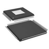
ADAU1445YSVZ-3A-RL Analog Devices Inc, ADAU1445YSVZ-3A-RL Datasheet - Page 37

ADAU1445YSVZ-3A-RL
Manufacturer Part Number
ADAU1445YSVZ-3A-RL
Description
175MHZ SigmaDSP,2x8 SRCs
Manufacturer
Analog Devices Inc
Series
SigmaDSP®r
Type
Audio Processorr
Specifications of ADAU1445YSVZ-3A-RL
Applications
Automotive Audio
Mounting Type
Surface Mount
Package / Case
100-TQFP Exposed Pad, 100-eTQFP, 100-HTQFP, 100-VQFP
Format
Fixed Point
Program Memory Size
Not RequiredKB
Operating Supply Voltage (typ)
1.8/3.3V
Operating Temp Range
-40C to 105C
Operating Temperature Classification
Industrial
Mounting
Surface Mount
Pin Count
100
Lead Free Status / RoHS Status
Lead free / RoHS Compliant
Lead Free Status / RoHS Status
Lead free / RoHS Compliant
Available stocks
Company
Part Number
Manufacturer
Quantity
Price
Company:
Part Number:
ADAU1445YSVZ-3A-RL
Manufacturer:
Analog Devices Inc
Quantity:
10 000
SERIAL INPUT PORT MODES AND SETTINGS
Each of the nine serial input ports is controlled by setting an
individual 2-byte word in the serial input mode register for each
port (see Table 23 for the register addresses). Each serial data
signal can be set to use any of the nine clock domains (slave
mode) or an internally generated LRCLK signal at f
f
set to stereo, I
slave mode using a 50% duty cycle LRCLK (as opposed to a
synchronization pulse). This configuration corresponds to a
setting of 0x3C00. The serial data uses its corresponding clock
domain (that is, SDATA3 uses LRCLK3 and BCLK3).
Restrictions
When in MOST mode (packed TDM4 mode), the MSB position
of the serial data must be delayed by one bit clock from the start
of the frame (I
Each channel has a frame of 32 bits. Therefore, when in delay-
by-12 mode, the serial data can only be 16 or 20 bits wide (not
Table 24. Bit Descriptions of Serial Input Port Modes Registers
Bit Position
[15]
[14]
[13:10]
[9]
[8]
S,DUAL
, or f
S,QUAD
2
S, 24-bit, negative LRCLK and BCLK polarity,
2
S position) and the data must be 16 bits wide
. The default value for each serial port on reset is
Description
Clock output enable
0 = LRCLK and BCLK output pins disabled
1 = LRCLK and BCLK output pins enabled
Frame sync type
0 = LRCLK 50/50 duty cycle clock signal (square wave)
1 = LRCLK synchronization pulse (narrow pulse)
Clock domain master/slave select
0000 = slave to Clock Domain 0 (Port 1)
0001 = slave to Clock Domain 1 (Port 2)
0010 = slave to Clock Domain 2 (Port 3)
0011 = slave to Clock Domain 3 (Port 4)
0100 = slave to Clock Domain 4 (Port 5)
0101 = slave to Clock Domain 5 (Port 6
0110 = slave to Clock Domain 6 (Port 7)
0111 = slave to Clock Domain 7 (Port 8)
1000 = slave to Clock Domain 8 (Port 9)
1001 = master, clock is f
1010 = master, clock is f
1011 = master, clock is f
Serial input BCLK polarity
0 = negative BCLK polarity
1 = positive BCLK polarity
Serial input LRCLK polarity
0 = negative BCLK polarity
1 = positive BCLK polarity
1
S,NORMAL
S,DUAL
S,QUAD
S,NORMAL
1
,
Rev. A | Page 37 of 92
24 bits). When in delay-by-16 mode, the serial data can only be
16 bits wide.
Due to the limited maximum clock speed, master and slave modes
are only compatible with certain TDM modes. See Table 16 for
more details.
Serial Input Port Modes Registers (Address 0xE000 to
Address 0xE008)
Table 23. Addresses of Serial Input Port Modes Registers
Decimal
57344
57345
57346
57347
57348
57349
57350
57351
57352
Address
Hex
E000
E001
E002
E003
E004
E005
E006
E007
E008
Name
Serial Input Port 0 modes
Serial Input Port 1 modes
Serial Input Port 2 modes
Serial Input Port 3 modes
Serial Input Port 4 modes
Serial Input Port 5 modes
Serial Input Port 6 modes
Serial Input Port 7 modes
Serial Input Port 8 modes
ADAU1445/ADAU1446
Default
0
0
Address specific
0
0
Read/Write
Word Length
16 bits (2 bytes)
16 bits (2 bytes)
16 bits (2 bytes)
16 bits (2 bytes)
16 bits (2 bytes)
16 bits (2 bytes)
16 bits (2 bytes)
16 bits (2 bytes)
16 bits (2 bytes)
2


