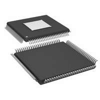
ADAU1445YSVZ-3A-RL Analog Devices Inc, ADAU1445YSVZ-3A-RL Datasheet - Page 25

ADAU1445YSVZ-3A-RL
Manufacturer Part Number
ADAU1445YSVZ-3A-RL
Description
175MHZ SigmaDSP,2x8 SRCs
Manufacturer
Analog Devices Inc
Series
SigmaDSP®r
Type
Audio Processorr
Specifications of ADAU1445YSVZ-3A-RL
Applications
Automotive Audio
Mounting Type
Surface Mount
Package / Case
100-TQFP Exposed Pad, 100-eTQFP, 100-HTQFP, 100-VQFP
Format
Fixed Point
Program Memory Size
Not RequiredKB
Operating Supply Voltage (typ)
1.8/3.3V
Operating Temp Range
-40C to 105C
Operating Temperature Classification
Industrial
Mounting
Surface Mount
Pin Count
100
Lead Free Status / RoHS Status
Lead free / RoHS Compliant
Lead Free Status / RoHS Status
Lead free / RoHS Compliant
Available stocks
Company
Part Number
Manufacturer
Quantity
Price
Company:
Part Number:
ADAU1445YSVZ-3A-RL
Manufacturer:
Analog Devices Inc
Quantity:
10 000
the idle condition. The R/ W bit determines the direction of the
data. A Logic 0 on the LSB of the first byte means that the master
writes information to the peripheral. A Logic 1 on the LSB of
the first byte means that the master reads information from the
peripheral. A data transfer takes place until a stop condition is
encountered. A stop condition occurs when SDA transitions
from low to high while SCL is held high.
timing of an I
Burst mode addressing, where the subaddresses are automatically
incremented at word boundaries, can be used for writing large
amounts of data to contiguous memory locations. This increment
happens automatically, unless a stop condition is encountered after
a single-word write. The registers and RAMs in the ADAU1445/
ADAU1446 range in width from one to five bytes; therefore, the
auto-increment feature knows the mapping between subaddresses
and the word length of the destination register (or memory lo-
cation). A data transfer is always terminated by a stop condition.
Stop and start conditions can be detected at any stage during the
data transfer. If these conditions are asserted out of sequence
with normal read and write operations, they cause an immediate
jump to the idle condition. During a given SCL high period, the
user should only issue one start condition, one stop condition, or a
single stop condition followed by a single start condition. If an in-
valid subaddress is issued by the user, the ADAU1445/ADAU1446
do not issue an acknowledge and return to the idle condition. If
the user exceeds the highest subaddress while in auto-increment
mode, one of two actions is taken. In read mode, the ADAU1445/
ADAU1446 output the highest subaddress register contents
until the master device issues a no acknowledge, indicating the
end of a read. A no-acknowledge condition is where the SDA
line is not pulled low on the ninth clock pulse on SCL. If the
highest subaddress location is reached while in write mode, the
data for the invalid byte is not loaded into any subaddress register, a
(CONTINUED)
(CONTINUED)
START BY
MASTER
SCL
SDA
SCL
SDA
2
C write.
0
1
1
CHI P ADDRESS BYTE
SUBADDRESS BYTE 2
1
FRAME 1
Figure 13
FRAME 2
0
shows the
0
ADAU1445/ADAU1446
ADAU1445/ADAU1446
ADR
SEL
Figure 13. I
Rev. A | Page 25 of 92
R/W
ACK BY
ACK BY
2
C Write Clocking
no acknowledge is issued by the ADAU1445/ADAU1446, and
the part returns to the idle condition.
I
Figure 15 shows the sequence of a single-word write operation.
Every ninth clock, the ADAU1445/ADAU1446 issue an
acknowledge by pulling SDA low.
Figure 16 shows the sequence of a burst mode write operation.
This figure shows an example in which the target destination
registers are two bytes. The ADAU1445/ADAU1446 know to
increment the subaddress register every two bytes because the
requested subaddress corresponds to a register or memory area
with a 2-byte word length.
The sequence of a single-word read operation is shown in
Figure 17. Note that, even though this is a read operation, the
first R/ W bit is a 0, indicating a write operation. This is because
the subaddress must be written to set up the internal address.
After the ADAU1445/ADAU1446 acknowledge the receipt of
the subaddress, the master must issue a repeated start command
followed by the chip address byte with the R/ W set to 1, indicating
a read operation. This causes the SDA pin of the ADAU1445/
ADAU1446 to switch directions and begin driving data back to
the master. The master then responds every ninth pulse with an
acknowledge pulse to the ADAU1445/ADAU1446.
Figure 18 shows the sequence of a burst mode read operation.
This figure shows an example in which the target read registers
are two bytes. The ADAU1445/ADAU1446 increment the
subaddress every two bytes because the requested subaddress
corresponds to a register or memory area with word lengths of
two bytes. Other address ranges can have a variety of word
lengths, ranging from one to five bytes; the ADAU1445/
ADAU1446 always decode the subaddress and set the auto-
increment circuit so that the address increments after the
appropriate number of bytes.
2
C Read and Write Operations
SUBADDRESS BYTE 1
DATA BYTE 1
FRAME 3
FRAME 2
ADAU1445/ADAU1446
ADAU1445/ADAU1446
ADAU1445/ADAU1446
ACK BY
ACK BY
STOP BY
MASTER


