ADAU1445YSVZ-3A-RL Analog Devices Inc, ADAU1445YSVZ-3A-RL Datasheet - Page 35
ADAU1445YSVZ-3A-RL
Manufacturer Part Number
ADAU1445YSVZ-3A-RL
Description
175MHZ SigmaDSP,2x8 SRCs
Manufacturer
Analog Devices Inc
Series
SigmaDSP®r
Type
Audio Processorr
Specifications of ADAU1445YSVZ-3A-RL
Applications
Automotive Audio
Mounting Type
Surface Mount
Package / Case
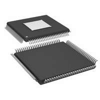
100-TQFP Exposed Pad, 100-eTQFP, 100-HTQFP, 100-VQFP
Format
Fixed Point
Program Memory Size
Not RequiredKB
Operating Supply Voltage (typ)
1.8/3.3V
Operating Temp Range
-40C to 105C
Operating Temperature Classification
Industrial
Mounting
Surface Mount
Pin Count
100
Lead Free Status / RoHS Status
Lead free / RoHS Compliant
Lead Free Status / RoHS Status
Lead free / RoHS Compliant
Available stocks
Company
Part Number
Manufacturer
Quantity
Price
Company:

Part Number:
ADAU1445YSVZ-3A-RL
Manufacturer:
Analog Devices Inc
Quantity:
10 000


SERIAL INPUT PORTS
The serial input ports convert standard I
16-, 20-, and 24-bit audio signals for input to the audio processor.
They support TDM2, TDM4, TDM8, and TDM16 time division
multiplexing schemes and I
delay-by-12 and delay-by-16 modes. Different clock polarities
and multiple word lengths are supported, as well as the capability
to drive in master mode or to be driven in slave mode.
The serial input ports are composed of up to nine clock domains
(Clock Domain 0 to Clock Domain 8) and up to nine serial data
signals (SDATA_IN0 to SDATA_IN8).
In slave mode, the nine serial input clock domains are driven
directly from the corresponding nine pairs of LRCLKx and
BCLKx pins on the IC. Three pairs of LRCLKx and BCLKx pins
(LRCLK[2:0] and BCLK[2:0]) are hardwired to Clock
Domains[2:0], which are serial inputs. The remaining six pairs
of LRCLKx and BCLKx pins (LRCLK[8:3] and BCLK[8:3]) are
multiplexed to Clock Domains[8:3] as either inputs or outputs.
The multiplexer can be set to use these signals as input clock
domains by writing to Bits[5:0] of the clock pad multiplexer
register (Address 0xE240) as explained in Table 21. This
configuration is also valid in master mode.
Figure 30 shows in more detail how the clocks are routed to and
from the serial input ports. For the assignable clock domains
(Clock Domains[8:3]), the clock pad multiplexer allows them to
be routed either to the serial input ports or to the serial output
ports independently. In slave mode, the clock domain selector
(that is, the 18:2 multiplexer) allows each serial input port to
clock from any available clock domain. In master mode, the
2
S, left-justified, right-justified, MSB
2
S and TDM signals into
Rev. A | Page 35 of 92
clock domain selector is bypassed, and the assignments described
in Table 22 are used.
The maximum number of audio channels that can be input to
SigmaDSP is 24. The serial input ports must be set in a way that
respects this (for example, two TDM16 streams is not a valid entry).
Table 21. Input Clock Domain Multiplexing
Clock Domain
0
1
2
3
4
5
6
7
8
Table 22. Input Clock Domain Assignments in Master Mode
Data Pin
SDATA_IN0
SDATA_IN1
SDATA_IN2
SDATA_IN3
SDATA_IN4
SDATA_IN5
SDATA_IN6
SDATA_IN7
SDATA_IN8
Chip Pins
LRCLK0, BCLK0
LRCLK1, BCLK1
LRCLK2, BCLK2
LRCLK3, BCLK3
LRCLK4, BCLK4
LRCLK5, BCLK5
LRCLK6, BCLK6
LRCLK7, BCLK7
LRCLK8, BCLK8
Clock Pins
LRCLK0, BCLK0
LRCLK1, BCLK1
LRCLK2, BCLK2
LRCLK3, BCLK3
LRCLK4, BCLK4
LRCLK5, BCLK5
LRCLK6, BCLK6
LRCLK7, BCLK7
LRCLK8, BCLK8
ADAU1445/ADAU1446
Register 0xE240 Setting
N/A
N/A
N/A
Set Bit 0 to 0
Set Bit 1 to 0
Set Bit 2 to 0
Set Bit 3 to 0
Set Bit 4 to 0
Set Bit 5 to 0
Related parts for ADAU1445YSVZ-3A-RL
Image
Part Number
Description
Manufacturer
Datasheet
Request
R

Part Number:
Description:
SigmaDSP� Digital Audio Processor with Flexible Audio Routing Matrix
Manufacturer:
Analog Devices
Datasheet:

Part Number:
Description:
±1.7g Dual-Axis IMEMS Accelerometer Evaluation Board
Manufacturer:
Analog Devices Inc
Datasheet:

Part Number:
Description:
Inertial Sensor Evaluation System
Manufacturer:
Analog Devices Inc
Datasheet:
Part Number:
Description:
Manufacturer:
Analog Devices Inc
Datasheet:
Part Number:
Description:
Manufacturer:
Analog Devices Inc
Datasheet:
Part Number:
Description:
Manufacturer:
Analog Devices Inc
Datasheet:
Part Number:
Description:
Manufacturer:
Analog Devices Inc
Datasheet:
Part Number:
Description:
Manufacturer:
Analog Devices Inc
Datasheet:
Part Number:
Description:
Manufacturer:
Analog Devices Inc
Datasheet:
Part Number:
Description:
Manufacturer:
Analog Devices Inc
Datasheet:
Part Number:
Description:
Manufacturer:
Analog Devices Inc
Datasheet:
Part Number:
Description:
Manufacturer:
Analog Devices Inc
Datasheet:
Part Number:
Description:
Manufacturer:
Analog Devices Inc
Datasheet: