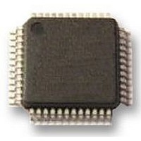
UPD78F0413GA-GAM-AX NEC, UPD78F0413GA-GAM-AX Datasheet - Page 387

UPD78F0413GA-GAM-AX
Manufacturer Part Number
UPD78F0413GA-GAM-AX
Description
8BIT UC, 32K FLASH, 1KB RAM, LCD
Manufacturer
NEC
Datasheet
1.UPD78F0413GA-GAM-AX.pdf
(562 pages)
Specifications of UPD78F0413GA-GAM-AX
Controller Family/series
UPD78F
No. Of I/o's
30
Ram Memory Size
1024Byte
Cpu Speed
10MHz
No. Of Timers
8
No. Of Pwm
RoHS Compliant
Core Size
8bit
Program Memory Size
32KB
Oscillator Type
External, Internal
Available stocks
Company
Part Number
Manufacturer
Quantity
Price
Company:
Part Number:
UPD78F0413GA-GAM-AX
Manufacturer:
ADI
Quantity:
882
Company:
Part Number:
UPD78F0413GA-GAM-AX
Manufacturer:
Renesas Electronics America
Quantity:
10 000
- Current page: 387 of 562
- Download datasheet (4Mb)
15.6 Common and Segment Signals
segment signals becomes higher than a specific voltage (LCD drive voltage, V
potential difference becomes lower than V
problem, this LCD panel is driven by AC voltage.
Each pixel of the LCD panel turns on when the potential difference between the corresponding common and
Applying DC voltage to the common and segment signals of an LCD panel causes deterioration. To avoid this
(1)
(2)
Number of
Time Slices
eight-time-slice mode
Static display mode
Two-time-slice mode
Three-time-slice mode
Four-time-slice mode
Common signals
Each common signal is selected sequentially according to a specified number of time slices at the timing
listed in Table 15-3. In the static display mode, the same signal is output to COM0 to COM3.
In the two-time-slice mode, leave the COM2 and COM3 pins open. In the three-time-slice mode, leave the
COM3 pin open.
Use the COM4 to COM7 pins other than in the eight-time-slice mode as open or segment pins.
Note
Segment signals
The segment signals correspond to 22 bytes of LCD display data memory (FA40H to FA55H). Bits 0, 1, 2,
and 3 of each byte are read in synchronization with COM0, COM1, COM2, and COM3, respectively. If a bit is
1, it is converted to the select voltage, and if it is 0, it is converted to the deselect voltage. The conversion
results are output to the segment pins (SEG0 to SEG21).
Check, with the information given above, what combination of front-surface electrodes (corresponding to the
segment signals) and rear-surface electrodes (corresponding to the common signals) forms display patterns
in the LCD display data memory, and write the bit data that corresponds to the desired display pattern on a
one-to-one basis.
LCD display data memory bits 1 to 3, bits 2 and 3, and bit 3 are not used for LCD display in the static display,
two-time slot, and three-time slot modes, respectively. So these bits can be used for purposes other than
display.
The higher 4 bits of FA40H to FA43H are fixed to 0.
COM Signal
Use the pins as open or segment pins.
COM0
CHAPTER 15 LCD CONTROLLER/DRIVER
COM1
LCD
.
Table 15-3. COM Signals
User’s Manual U18698EJ1V0UD
Open
COM2
Open
Open
COM3
COM4
Note
Note
Note
Note
LCD
). The pixels turn off when the
COM5
Note
Note
Note
Note
COM6
Note
Note
Note
Note
COM7
Note
Note
Note
Note
387
Related parts for UPD78F0413GA-GAM-AX
Image
Part Number
Description
Manufacturer
Datasheet
Request
R

Part Number:
Description:
16/8 bit single-chip microcomputer
Manufacturer:
NEC
Datasheet:

Part Number:
Description:
Dual audio power amp circuit
Manufacturer:
NEC
Datasheet:

Part Number:
Description:
Dual comparator
Manufacturer:
NEC
Datasheet:

Part Number:
Description:
MOS type composite field effect transistor
Manufacturer:
NEC
Datasheet:

Part Number:
Description:
50 V/100 mA FET array incorporating 2 N-ch MOSFETs
Manufacturer:
NEC
Datasheet:

Part Number:
Description:
6-pin small MM high-frequency double transistor
Manufacturer:
NEC
Datasheet:

Part Number:
Description:
6-pin small MM high-frequency double transistor
Manufacturer:
NEC
Datasheet:

Part Number:
Description:
6-pin small MM high-frequency double transistor
Manufacturer:
NEC
Datasheet:

Part Number:
Description:
6-pin small MM high-frequency double transistor
Manufacturer:
NEC
Datasheet:

Part Number:
Description:
Twin transistors equipped with different model chips(6P small MM)
Manufacturer:
NEC
Datasheet:

Part Number:
Description:
Bipolar analog integrated circuit
Manufacturer:
NEC
Datasheet:


