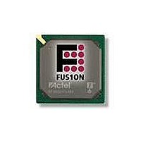
AFS600-FGG256 Actel, AFS600-FGG256 Datasheet - Page 81

AFS600-FGG256
Manufacturer Part Number
AFS600-FGG256
Description
FPGA - Field Programmable Gate Array 600K System Gates
Manufacturer
Actel
Datasheet
1.AFS600-PQG208.pdf
(330 pages)
Specifications of AFS600-FGG256
Processor Series
AFS600
Core
IP Core
Maximum Operating Frequency
1098.9 MHz
Number Of Programmable I/os
119
Data Ram Size
110592
Supply Voltage (max)
1.575 V
Maximum Operating Temperature
+ 70 C
Minimum Operating Temperature
0 C
Development Tools By Supplier
AFS-Eval-Kit, AFS-BRD600, FlashPro 3, FlashPro Lite, Silicon-Explorer II, Silicon-Sculptor 3, SI-EX-TCA
Mounting Style
SMD/SMT
Supply Voltage (min)
1.425 V
Number Of Gates
600 K
Package / Case
FPBGA-256
Lead Free Status / RoHS Status
Lead free / RoHS Compliant
Available stocks
Company
Part Number
Manufacturer
Quantity
Price
Company:
Part Number:
AFS600-FGG256
Manufacturer:
Actel
Quantity:
135
Part Number:
AFS600-FGG256
Manufacturer:
ACTEL/爱特
Quantity:
20 000
Company:
Part Number:
AFS600-FGG256I
Manufacturer:
Microsemi SoC
Quantity:
10 000
Company:
Part Number:
AFS600-FGG256K
Manufacturer:
Microsemi SoC
Quantity:
10 000
- Current page: 81 of 330
- Download datasheet (13Mb)
Modes of Operation
There are two read modes and one write mode:
RAM Initialization
Each SRAM block can be individually initialized on power-up by means of the JTAG port using the
UJTAG mechanism (refer to the
Blocks
bit configuration to enable serial loading. The 4,608 bits of data can be loaded in a single operation.
•
•
•
Read Nonpipelined (synchronous—1 clock edge): In the standard read mode, new data is driven
onto the RD bus in the same clock cycle following RA and REN valid. The read address is
registered on the read port clock active edge, and data appears at RD after the RAM access time.
Setting PIPE to OFF enables this mode.
Read Pipelined (synchronous—2 clock edges): The pipelined mode incurs an additional clock
delay from the address to the data but enables operation at a much higher frequency. The read
address is registered on the read port active clock edge, and the read data is registered and
appears at RD after the second read clock edge. Setting PIPE to ON enables this mode.
Write (synchronous—1 clock edge): On the write clock active edge, the write data is written into
the SRAM at the write address when WEN is High. The setup times of the write address, write
enables, and write data are minimal with respect to the write clock. Write and read transfers are
described with timing requirements in the
"FIFO Characteristics" section on page
application note). The shift register for a target block can be selected and loaded with the proper
"JTAG IEEE 1532" section on page 2-230
R e v i s i o n 1
2-77.
"SRAM Characteristics" section on page 2-66
Actel Fusion Family of Mixed Signal FPGAs
and the
Fusion SRAM/FIFO
and the
2- 65
Related parts for AFS600-FGG256
Image
Part Number
Description
Manufacturer
Datasheet
Request
R

Part Number:
Description:
AFS600-1FGG256I
Manufacturer:
Actel
Datasheet:

Part Number:
Description:
AFS600-2FGG256I
Manufacturer:
Actel
Datasheet:


