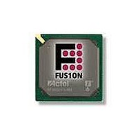
AFS600-FGG256 Actel, AFS600-FGG256 Datasheet - Page 157

AFS600-FGG256
Manufacturer Part Number
AFS600-FGG256
Description
FPGA - Field Programmable Gate Array 600K System Gates
Manufacturer
Actel
Datasheet
1.AFS600-PQG208.pdf
(330 pages)
Specifications of AFS600-FGG256
Processor Series
AFS600
Core
IP Core
Maximum Operating Frequency
1098.9 MHz
Number Of Programmable I/os
119
Data Ram Size
110592
Supply Voltage (max)
1.575 V
Maximum Operating Temperature
+ 70 C
Minimum Operating Temperature
0 C
Development Tools By Supplier
AFS-Eval-Kit, AFS-BRD600, FlashPro 3, FlashPro Lite, Silicon-Explorer II, Silicon-Sculptor 3, SI-EX-TCA
Mounting Style
SMD/SMT
Supply Voltage (min)
1.425 V
Number Of Gates
600 K
Package / Case
FPBGA-256
Lead Free Status / RoHS Status
Lead free / RoHS Compliant
Available stocks
Company
Part Number
Manufacturer
Quantity
Price
Company:
Part Number:
AFS600-FGG256
Manufacturer:
Actel
Quantity:
135
Part Number:
AFS600-FGG256
Manufacturer:
ACTEL/爱特
Quantity:
20 000
Company:
Part Number:
AFS600-FGG256I
Manufacturer:
Microsemi SoC
Quantity:
10 000
Company:
Part Number:
AFS600-FGG256K
Manufacturer:
Microsemi SoC
Quantity:
10 000
- Current page: 157 of 330
- Download datasheet (13Mb)
Double Data Rate (DDR) Support
Fusion Pro I/Os support 350 MHz DDR inputs and outputs. In DDR mode, new data is present on every
transition of the clock signal. Clock and data lines have identical bandwidths and signal integrity
requirements, making it very efficient for implementing very high-speed systems.
DDR interfaces can be implemented using HSTL, SSTL, LVDS, and LVPECL I/O standards. In addition,
high-speed DDR interfaces can be implemented using LVDS I/O.
Input Support for DDR
The basic structure to support a DDR input is shown in
capture incoming data, which is presented to the core on each rising edge of the I/O register clock.
Each I/O tile on Fusion devices supports DDR inputs.
Output Support for DDR
The basic DDR output structure is shown in
output every half clock cycle. Note: DDR macros and I/O registers do not require additional routing. The
combiner automatically recognizes the DDR macro and pushes its registers to the I/O register area at the
edge of the chip. The routing delay from the I/O registers to the I/O buffers is already taken into account
in the DDR macro.
Refer to the Actel application note
Figure 2-99 • DDR Input Register Support in Fusion Devices
Data
CLK
CLR
INBUF
INBUF
CLKBUF
A
B
C
Using DDR for Fusion Devices
R e v i s i o n 1
Figure 2-100 on page
DDR_IN
Input DDR
Figure
FF1
2-99. Three input registers are used to
FF2
Actel Fusion Family of Mixed Signal FPGAs
for more information.
2-142. New data is presented to the
D
E
Out_QF
(to core)
Out_QR
(to core)
2- 141
Related parts for AFS600-FGG256
Image
Part Number
Description
Manufacturer
Datasheet
Request
R

Part Number:
Description:
AFS600-1FGG256I
Manufacturer:
Actel
Datasheet:

Part Number:
Description:
AFS600-2FGG256I
Manufacturer:
Actel
Datasheet:


